ST72F344K4T6 STMicroelectronics, ST72F344K4T6 Datasheet - Page 152
ST72F344K4T6
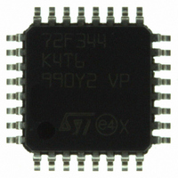
Manufacturer Part Number
ST72F344K4T6
Description
MCU 8BIT 16KB FLASH MEM 32-LQFP
Manufacturer
STMicroelectronics
Series
ST7r
Datasheet
1.ST72F344K2T6.pdf
(247 pages)
Specifications of ST72F344K4T6
Core Processor
ST7
Core Size
8-Bit
Speed
8MHz
Connectivity
I²C, LIN, SCI, SPI
Peripherals
LVD, POR, PWM, WDT
Number Of I /o
24
Program Memory Size
16KB (16K x 8)
Program Memory Type
FLASH
Eeprom Size
256 x 8
Ram Size
1K x 8
Voltage - Supply (vcc/vdd)
2.7 V ~ 5.5 V
Data Converters
A/D 12x10b
Oscillator Type
Internal
Operating Temperature
-40°C ~ 85°C
Package / Case
32-LQFP
Processor Series
ST72F3x
Core
ST7
Data Bus Width
8 bit
Data Ram Size
1 KB
Interface Type
I2C, SCI, SPI
Maximum Clock Frequency
8 MHz
Number Of Programmable I/os
34
Number Of Timers
2
Maximum Operating Temperature
+ 85 C
Mounting Style
SMD/SMT
Development Tools By Supplier
ST72F34X-SK/RAIS, ST7MDT40-EMU3, STX-RLINK
Minimum Operating Temperature
- 40 C
On-chip Adc
10 bit, 8 Channel
For Use With
497-5046 - KIT TOOL FOR ST7/UPSD/STR7 MCU
Lead Free Status / RoHS Status
Lead free / RoHS Compliant
Other names
497-5611
Available stocks
Company
Part Number
Manufacturer
Quantity
Price
Company:

Part Number:
ST72F344K4T6
Manufacturer:
STMicroelectronics
Quantity:
10 000
Company:
Part Number:
ST72F344K4T6TR
Manufacturer:
STMicroelectronics
Quantity:
10 000


On-chip peripherals
11.6.4
Note:
152/247
When the I
In this case, the value of the external pull-up resistor used depends on the application.
When the I
Figure 68.
Functional description
Refer to the CR, SR1 and SR2 registers in
By default the I
initiates a transmit or receive sequence.
First the interface frequency must be configured using the FRi bits in the OAR2 register.
Slave mode
As soon as a start condition is detected, the address is received from the SDA line and sent
to the shift register; then it is compared with the address of the interface or the General Call
address (if selected by software).
In 10-bit addressing mode, the comparison includes the header sequence (11110xx0) and
the two most significant bits of the address.
Header matched (10-bit mode only): the interface generates an acknowledge pulse if the
ACK bit is set.
SDA or SDAI
SCL or SCLI
2
2
C cell is enabled, the SDA and SCL ports must be configured as floating inputs.
C cell is disabled, the SDA and SCL ports revert to being standard I/O port pins.
I
2
2
C interface block diagram
C interface operates in Slave mode (M/SL bit is cleared) except when it
Clock control
Clock control register (CCR)
Status register 1 (SR1)
Status register 2 (SR2)
Data control
Control register (CR)
Doc ID 12321 Rev 5
Section
Own address register 1 (OAR1)
Own address register 2 (OAR2)
11.6.7. for the bit definitions.
Data register (DR)
Data shift register
Control logic
Comparator
Interrupt
ST72344xx ST72345xx
Related parts for ST72F344K4T6
Image
Part Number
Description
Manufacturer
Datasheet
Request
R

Part Number:
Description:
STMicroelectronics [RIPPLE-CARRY BINARY COUNTER/DIVIDERS]
Manufacturer:
STMicroelectronics
Datasheet:
Part Number:
Description:
STMicroelectronics [LIQUID-CRYSTAL DISPLAY DRIVERS]
Manufacturer:
STMicroelectronics
Datasheet:

Part Number:
Description:
BOARD EVAL FOR MEMS SENSORS
Manufacturer:
STMicroelectronics
Datasheet:
Part Number:
Description:
NPN TRANSISTOR POWER MODULE
Manufacturer:
STMicroelectronics
Datasheet:
Part Number:
Description:
TURBOSWITCH ULTRA-FAST HIGH VOLTAGE DIODE
Manufacturer:
STMicroelectronics
Datasheet:
Part Number:
Description:
Manufacturer:
STMicroelectronics
Datasheet:
Part Number:
Description:
DIODE / SCR MODULE
Manufacturer:
STMicroelectronics
Datasheet:
Part Number:
Description:
DIODE / SCR MODULE
Manufacturer:
STMicroelectronics
Datasheet:
Part Number:
Description:
Search -----> STE16N100
Manufacturer:
STMicroelectronics
Datasheet:
Part Number:
Description:
Search ---> STE53NA50
Manufacturer:
STMicroelectronics
Datasheet:
Part Number:
Description:
NPN Transistor Power Module
Manufacturer:
STMicroelectronics
Datasheet:
Part Number:
Description:
DIODE / SCR MODULE
Manufacturer:
STMicroelectronics
Datasheet: