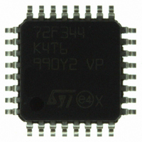
ST72F344K4T6 STMicroelectronics, ST72F344K4T6 Datasheet - Page 139

ST72F344K4T6
Manufacturer Part Number
ST72F344K4T6
Description
MCU 8BIT 16KB FLASH MEM 32-LQFP
Manufacturer
STMicroelectronics
Series
ST7r
Datasheet
1.ST72F344K2T6.pdf
(247 pages)
Specifications of ST72F344K4T6
Core Processor
ST7
Core Size
8-Bit
Speed
8MHz
Connectivity
I²C, LIN, SCI, SPI
Peripherals
LVD, POR, PWM, WDT
Number Of I /o
24
Program Memory Size
16KB (16K x 8)
Program Memory Type
FLASH
Eeprom Size
256 x 8
Ram Size
1K x 8
Voltage - Supply (vcc/vdd)
2.7 V ~ 5.5 V
Data Converters
A/D 12x10b
Oscillator Type
Internal
Operating Temperature
-40°C ~ 85°C
Package / Case
32-LQFP
Processor Series
ST72F3x
Core
ST7
Data Bus Width
8 bit
Data Ram Size
1 KB
Interface Type
I2C, SCI, SPI
Maximum Clock Frequency
8 MHz
Number Of Programmable I/os
34
Number Of Timers
2
Maximum Operating Temperature
+ 85 C
Mounting Style
SMD/SMT
Development Tools By Supplier
ST72F34X-SK/RAIS, ST7MDT40-EMU3, STX-RLINK
Minimum Operating Temperature
- 40 C
On-chip Adc
10 bit, 8 Channel
For Use With
497-5046 - KIT TOOL FOR ST7/UPSD/STR7 MCU
Lead Free Status / RoHS Status
Lead free / RoHS Compliant
Other names
497-5611
Available stocks
Company
Part Number
Manufacturer
Quantity
Price
Company:
Part Number:
ST72F344K4T6
Manufacturer:
STMicroelectronics
Quantity:
10 000
Company:
Part Number:
ST72F344K4T6TR
Manufacturer:
STMicroelectronics
Quantity:
10 000
ST72344xx ST72345xx
Note:
Setting the RWU bit by software puts the SCI in sleep mode:
●
●
A muted receiver can be woken up in one of the following two ways:
●
●
A receiver wakes-up by Idle Line detection when the Receive line has recognized an Idle
Frame. Then the RWU bit is reset by hardware but the IDLE bit is not set.
A receiver wakes-up by Address Mark detection when it received a “1” as the most
significant bit of a word, thus indicating that the message is an address. The reception of
this particular word wakes up the receiver, resets the RWU bit and sets the RDRF bit, which
allows the receiver to receive this word normally and to use it as an address word.
Parity control
Parity control (generation of parity bit in transmission and parity checking in reception) can
be enabled by setting the PCE bit in the SCICR1 register. Depending on the frame length
defined by the M bit, the possible SCI frame formats are as listed in
Table 56.
1. SB: Start Bit, STB: Stop Bit, PB: Parity Bit.
In case of wakeup by an address mark, the MSB bit of the data is taken into account and not
the parity bit
Even parity: The parity bit is calculated to obtain an even number of “1s” inside the frame
made of the 7 or 8 LSB bits (depending on whether M is equal to 0 or 1) and the parity bit.
Example: data = 00110101; 4 bits set => parity bit is 0 if even parity is selected (PS bit = 0).
Odd parity: The parity bit is calculated to obtain an odd number of “1s” inside the frame
made of the 7 or 8 LSB bits (depending on whether M is equal to 0 or 1) and the parity bit.
Example: data = 00110101; 4 bits set => parity bit is 1 if odd parity is selected (PS bit = 1).
Transmission mode: If the PCE bit is set then the MSB bit of the data written in the data
register is not transmitted but is changed by the parity bit.
Reception mode: If the PCE bit is set then the interface checks if the received data byte
has an even number of “1s” if even parity is selected (PS = 0) or an odd number of “1s” if
odd parity is selected (PS = 1). If the parity check fails, the PE flag is set in the SCISR
register and an interrupt is generated if PIE is set in the SCICR1 register.
0
1
M bit
None of the reception status bits can be set.
All the receive interrupts are inhibited.
by Idle Line detection if the WAKE bit is reset,
by Address Mark detection if the WAKE bit is set.
Frame formats
0
1
0
1
PCE bit
Doc ID 12321 Rev 5
| SB | 8 bit data | STB |
| SB | 7-bit data | PB | STB |
| SB | 9-bit data | STB |
| SB | 8-bit data PB | STB |
SCI frame
(1)
Table
On-chip peripherals
56.
139/247


