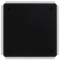
MCF5407AI220 Freescale Semiconductor, MCF5407AI220 Datasheet - Page 423

MCF5407AI220
Manufacturer Part Number
MCF5407AI220
Description
IC MPU 32B 220MHZ COLDF 208-FQFP
Manufacturer
Freescale Semiconductor
Series
MCF540xr
Specifications of MCF5407AI220
Core Processor
Coldfire V4
Core Size
32-Bit
Speed
220MHz
Connectivity
EBI/EMI, I²C, UART/USART
Peripherals
DMA, WDT
Number Of I /o
16
Program Memory Type
ROMless
Ram Size
4K x 8
Voltage - Supply (vcc/vdd)
1.65 V ~ 3.6 V
Oscillator Type
External
Operating Temperature
0°C ~ 70°C
Package / Case
208-FQFP
Maximum Clock Frequency
220 MHz
Operating Supply Voltage
1.8 V, 3.3 V
Maximum Operating Temperature
+ 105 C
Mounting Style
SMD/SMT
Minimum Operating Temperature
0 C
Program Memory Size
24KB
Cpu Speed
220MHz
Embedded Interface Type
I2C, UART
Digital Ic Case Style
FQFP
No. Of Pins
208
Supply Voltage Range
3.3V
Rohs Compliant
Yes
For Use With
M5407C3 - KIT EVAL FOR MCF5407 W/ETHERNET
Lead Free Status / RoHS Status
Lead free / RoHS Compliant
Eeprom Size
-
Program Memory Size
-
Data Converters
-
Lead Free Status / Rohs Status
Lead free / RoHS Compliant
Available stocks
Company
Part Number
Manufacturer
Quantity
Price
Company:
Part Number:
MCF5407AI220
Manufacturer:
freescaie
Quantity:
6
Company:
Part Number:
MCF5407AI220
Manufacturer:
Freescale Semiconductor
Quantity:
135
Company:
Part Number:
MCF5407AI220
Manufacturer:
FREESCALE
Quantity:
1 831
Company:
Part Number:
MCF5407AI220
Manufacturer:
Freescale Semiconductor
Quantity:
10 000
- Current page: 423 of 546
- Download datasheet (7Mb)
17.7.4 Synchronous DRAM Column Address Strobe (SCAS)
The synchronous DRAM column address strobe (SCAS) is registered during synchronous
mode to route directly to the SCAS signal of SDRAMs.
17.7.5 Synchronous DRAM Row Address Strobe (SRAS)
The synchronous DRAM row address strobe output (SRAS) is registered during
synchronous mode to route directly to the SRAS signal of external SDRAMs.
17.7.6 Synchronous DRAM Clock Enable (SCKE)
The synchronous DRAM clock enable output (SCKE) is registered during synchronous
mode to route directly to the SCKE signal of external SDRAMs. This signal provides the
clock enable to the SDRAM.
17.7.7 Synchronous Edge Select (EDGESEL)
The synchronous edge select input (EDGESEL) helps select additional output hold times
for signals that interface to external SDRAMs. It provides the following three modes of
operation for SDRAM control signals:
17.8 DMA Controller Module Signals
The DMA controller module uses the signals in the following subsections to provide
external request for either a source or destination.
17.8.1 DMA Request (DREQ[1:0]/PP[6:5])
The DMA request pins (DREQ[1:0]/PP[6:5]) can serve as the DMA request inputs or as
two bits of the parallel port, as determined by individually programmable bits in the PAR.
These inputs are asserted by a peripheral device to request an operand transfer between that
peripheral and memory by either channel 0 or 1 of the on-chip DMA.
• When EDGESEL is tied high, SDRAM control signals change on the rising edge of
• When EDGESEL is tied low, SDRAM control signals change on the falling edge of
• When EDGESEL is tied to the external clock (normally buffered CLKIN), which
CLKIN.
CLKIN.
drives the SDRAM and other devices, SDRAM signals are generated within the
MCF5407 make a transition on the rising edge of the SDRAM clock. See
Figure 11-14 on page 11-19. This loop-back configuration provides additional
output hold time for MCF5407 interface signals provided to the SDRAM. In this
case, the SDRAM clock operates at the CLKIN frequency, with a possible slight
phase delay.
Chapter 17. Signal Descriptions
DMA Controller Module Signals
17-17
Related parts for MCF5407AI220
Image
Part Number
Description
Manufacturer
Datasheet
Request
R
Part Number:
Description:
Mcf5407 Coldfire Integrated Microprocessor User
Manufacturer:
Freescale Semiconductor, Inc
Datasheet:
Part Number:
Description:
Manufacturer:
Freescale Semiconductor, Inc
Datasheet:
Part Number:
Description:
Manufacturer:
Freescale Semiconductor, Inc
Datasheet:
Part Number:
Description:
Manufacturer:
Freescale Semiconductor, Inc
Datasheet:
Part Number:
Description:
Manufacturer:
Freescale Semiconductor, Inc
Datasheet:
Part Number:
Description:
Manufacturer:
Freescale Semiconductor, Inc
Datasheet:
Part Number:
Description:
Manufacturer:
Freescale Semiconductor, Inc
Datasheet:
Part Number:
Description:
Manufacturer:
Freescale Semiconductor, Inc
Datasheet:
Part Number:
Description:
Manufacturer:
Freescale Semiconductor, Inc
Datasheet:
Part Number:
Description:
Manufacturer:
Freescale Semiconductor, Inc
Datasheet:
Part Number:
Description:
Manufacturer:
Freescale Semiconductor, Inc
Datasheet:
Part Number:
Description:
Manufacturer:
Freescale Semiconductor, Inc
Datasheet:
Part Number:
Description:
Manufacturer:
Freescale Semiconductor, Inc
Datasheet:
Part Number:
Description:
Manufacturer:
Freescale Semiconductor, Inc
Datasheet:
Part Number:
Description:
Manufacturer:
Freescale Semiconductor, Inc
Datasheet:


