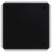
MCF5407AI220 Freescale Semiconductor, MCF5407AI220 Datasheet - Page 265

MCF5407AI220
Manufacturer Part Number
MCF5407AI220
Description
IC MPU 32B 220MHZ COLDF 208-FQFP
Manufacturer
Freescale Semiconductor
Series
MCF540xr
Specifications of MCF5407AI220
Core Processor
Coldfire V4
Core Size
32-Bit
Speed
220MHz
Connectivity
EBI/EMI, I²C, UART/USART
Peripherals
DMA, WDT
Number Of I /o
16
Program Memory Type
ROMless
Ram Size
4K x 8
Voltage - Supply (vcc/vdd)
1.65 V ~ 3.6 V
Oscillator Type
External
Operating Temperature
0°C ~ 70°C
Package / Case
208-FQFP
Maximum Clock Frequency
220 MHz
Operating Supply Voltage
1.8 V, 3.3 V
Maximum Operating Temperature
+ 105 C
Mounting Style
SMD/SMT
Minimum Operating Temperature
0 C
Program Memory Size
24KB
Cpu Speed
220MHz
Embedded Interface Type
I2C, UART
Digital Ic Case Style
FQFP
No. Of Pins
208
Supply Voltage Range
3.3V
Rohs Compliant
Yes
For Use With
M5407C3 - KIT EVAL FOR MCF5407 W/ETHERNET
Lead Free Status / RoHS Status
Lead free / RoHS Compliant
Eeprom Size
-
Program Memory Size
-
Data Converters
-
Lead Free Status / Rohs Status
Lead free / RoHS Compliant
Available stocks
Company
Part Number
Manufacturer
Quantity
Price
Company:
Part Number:
MCF5407AI220
Manufacturer:
freescaie
Quantity:
6
Company:
Part Number:
MCF5407AI220
Manufacturer:
Freescale Semiconductor
Quantity:
135
Company:
Part Number:
MCF5407AI220
Manufacturer:
FREESCALE
Quantity:
1 831
Company:
Part Number:
MCF5407AI220
Manufacturer:
Freescale Semiconductor
Quantity:
10 000
- Current page: 265 of 546
- Download datasheet (7Mb)
15–0
10.4.1.2 Chip-Select Mask Registers (CSMR0–CSMR7)
The chip select mask registers, Figure 10-3, are used to specify the address mask and
allowable access types for the respective chip selects.
Table 10-9 describes CSMR fields.
Bits
Reset
31–16
Field
Addr
R/W
.
Bits
8
7
6
31
Name
BA
Name
BAM
WP
AM
—
Base address. Defines the base address for memory dedicated to chip select CS[7:0]. BA is compared
to bits 31–16 on the internal address bus to determine if chip-select memory is being accessed.
Base address mask. Defines the chip select block by masking address bits. Setting a BAM bit
causes the corresponding CSAR bit to be ignored in the decode.
0 Corresponding address bit is used in chip-select decode.
1 Corresponding address bit is a don’t care in chip-select decode.
The block size for CS[7:0] is 2
So, if CSAR0 = 0x0000 and CSMR0[BAM] = 0x0008, CS0 would address two discontinuous
64-Kbyte memory blocks: one from 0x0000–0xFFFF and one from 0x8_0000–0x8_FFFF.
Likewise, for CS0 to access 32 Mbytes of address space starting at location 0x0, CS1 must begin
at the next byte after CS0 for a 16-Mbyte address space. Then CSAR0 = 0x0000,
CSMR0[BAM] = 0x01FF, CSAR1 = 0x0200, and CSMR1[BAM] = 0x00FF.
Write protect. Controls write accesses to the address range in the corresponding CSAR.
Attempting to write to the range of addresses for which CSARn[WP] = 1 results in the appropriate
chip select not being selected. No exception occurs.
0 Both read and write accesses are allowed.
1 Only read accesses are allowed.
Reserved, should be cleared.
Alternate master. When AM = 0 during an external master or DMA access, SC, SD, UC, and UD
are don’t cares in the chip-select decode.
Figure 10-3. Chip Select Mask Registers (CSMRn)
0x0B4 (CSMR4); 0x0C0 (CSMR5); 0x0CC (CSMR6); 0x0D8 (CSMR7)
0x084 (CSMR0); 0x090 (CSMR1); 0x09C (CSMR2); 0x0A8 (CSMR3);
BAM
Table 10-9. CSMRn Field Descriptions
Table 10-8. CSARn Field Description
Chapter 10. Chip-Select Module
n
; n = (number of bits set in respective CSMR[BAM]) + 16.
16 15
Unitialized
R/W
Description
Description
—
9
WP — AM C/I SC SD UC UD V
8
7
6
Chip-Select Registers
5
4
3
2
1
10-7
0
0
Related parts for MCF5407AI220
Image
Part Number
Description
Manufacturer
Datasheet
Request
R
Part Number:
Description:
Mcf5407 Coldfire Integrated Microprocessor User
Manufacturer:
Freescale Semiconductor, Inc
Datasheet:
Part Number:
Description:
Manufacturer:
Freescale Semiconductor, Inc
Datasheet:
Part Number:
Description:
Manufacturer:
Freescale Semiconductor, Inc
Datasheet:
Part Number:
Description:
Manufacturer:
Freescale Semiconductor, Inc
Datasheet:
Part Number:
Description:
Manufacturer:
Freescale Semiconductor, Inc
Datasheet:
Part Number:
Description:
Manufacturer:
Freescale Semiconductor, Inc
Datasheet:
Part Number:
Description:
Manufacturer:
Freescale Semiconductor, Inc
Datasheet:
Part Number:
Description:
Manufacturer:
Freescale Semiconductor, Inc
Datasheet:
Part Number:
Description:
Manufacturer:
Freescale Semiconductor, Inc
Datasheet:
Part Number:
Description:
Manufacturer:
Freescale Semiconductor, Inc
Datasheet:
Part Number:
Description:
Manufacturer:
Freescale Semiconductor, Inc
Datasheet:
Part Number:
Description:
Manufacturer:
Freescale Semiconductor, Inc
Datasheet:
Part Number:
Description:
Manufacturer:
Freescale Semiconductor, Inc
Datasheet:
Part Number:
Description:
Manufacturer:
Freescale Semiconductor, Inc
Datasheet:
Part Number:
Description:
Manufacturer:
Freescale Semiconductor, Inc
Datasheet:


