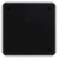
MCF5407AI220 Freescale Semiconductor, MCF5407AI220 Datasheet - Page 299

MCF5407AI220
Manufacturer Part Number
MCF5407AI220
Description
IC MPU 32B 220MHZ COLDF 208-FQFP
Manufacturer
Freescale Semiconductor
Series
MCF540xr
Specifications of MCF5407AI220
Core Processor
Coldfire V4
Core Size
32-Bit
Speed
220MHz
Connectivity
EBI/EMI, I²C, UART/USART
Peripherals
DMA, WDT
Number Of I /o
16
Program Memory Type
ROMless
Ram Size
4K x 8
Voltage - Supply (vcc/vdd)
1.65 V ~ 3.6 V
Oscillator Type
External
Operating Temperature
0°C ~ 70°C
Package / Case
208-FQFP
Maximum Clock Frequency
220 MHz
Operating Supply Voltage
1.8 V, 3.3 V
Maximum Operating Temperature
+ 105 C
Mounting Style
SMD/SMT
Minimum Operating Temperature
0 C
Program Memory Size
24KB
Cpu Speed
220MHz
Embedded Interface Type
I2C, UART
Digital Ic Case Style
FQFP
No. Of Pins
208
Supply Voltage Range
3.3V
Rohs Compliant
Yes
For Use With
M5407C3 - KIT EVAL FOR MCF5407 W/ETHERNET
Lead Free Status / RoHS Status
Lead free / RoHS Compliant
Eeprom Size
-
Program Memory Size
-
Data Converters
-
Lead Free Status / Rohs Status
Lead free / RoHS Compliant
Available stocks
Company
Part Number
Manufacturer
Quantity
Price
Company:
Part Number:
MCF5407AI220
Manufacturer:
freescaie
Quantity:
6
Company:
Part Number:
MCF5407AI220
Manufacturer:
Freescale Semiconductor
Quantity:
135
Company:
Part Number:
MCF5407AI220
Manufacturer:
FREESCALE
Quantity:
1 831
Company:
Part Number:
MCF5407AI220
Manufacturer:
Freescale Semiconductor
Quantity:
10 000
- Current page: 299 of 546
- Download datasheet (7Mb)
11.4.4.5 Auto-Refresh Operation
The DRAM controller is equipped with a refresh counter and control. This logic is
responsible for providing timing and control to refresh the SDRAM. Once the refresh
counter is set, and refresh is enabled, the counter counts to zero. At this time, an internal
refresh request flag is set and the counter begins counting down again. The DRAM
controller completes any active burst operation and then performs a
DRAM controller then initiates a refresh cycle and clears the refresh request flag. This
refresh cycle includes a delay from any precharge to the auto-refresh command, the
auto-refresh command, and then a delay until any
access initiated during the auto-refresh cycle is delayed until the cycle is completed.
Figure 11-22 shows the auto-refresh timing. In this case, there is an SDRAM access when
the refresh request becomes active. The request is delayed by the precharge to
programmed into the active SDRAM bank by the CAS bits. The
generated and the delay required by DCR[RTIM] is inserted before the next
command is generated. In this example, the next bus cycle is initiated, but does not generate
an SDRAM access until T
command, it is passed to both blocks of external SDRAM.
RAS[0] or [1]
Figure 11-21. Synchronous, Continuous Page-Mode Access—Read after Write
CAS[3:0]
DRAMW
D[31:0]
A[31:0]
CLKIN
SRAS
SCAS
ACTV
t
RCD
Row
Chapter 11. Synchronous/Asynchronous DRAM Controller Module
= 3
RC
NOP
is finished. Because both chip selects are active during the
WRITE
Column
NOP
ACTV
READ
command is allowed. Any SDRAM
Column
t
CASL
NOP
= 3
REF
NOP
Synchronous Operation
PALL
command is then
operation. The
NOP
t
EP
ACTV
PALL
delay
ACTV
11-31
REF
Related parts for MCF5407AI220
Image
Part Number
Description
Manufacturer
Datasheet
Request
R
Part Number:
Description:
Mcf5407 Coldfire Integrated Microprocessor User
Manufacturer:
Freescale Semiconductor, Inc
Datasheet:
Part Number:
Description:
Manufacturer:
Freescale Semiconductor, Inc
Datasheet:
Part Number:
Description:
Manufacturer:
Freescale Semiconductor, Inc
Datasheet:
Part Number:
Description:
Manufacturer:
Freescale Semiconductor, Inc
Datasheet:
Part Number:
Description:
Manufacturer:
Freescale Semiconductor, Inc
Datasheet:
Part Number:
Description:
Manufacturer:
Freescale Semiconductor, Inc
Datasheet:
Part Number:
Description:
Manufacturer:
Freescale Semiconductor, Inc
Datasheet:
Part Number:
Description:
Manufacturer:
Freescale Semiconductor, Inc
Datasheet:
Part Number:
Description:
Manufacturer:
Freescale Semiconductor, Inc
Datasheet:
Part Number:
Description:
Manufacturer:
Freescale Semiconductor, Inc
Datasheet:
Part Number:
Description:
Manufacturer:
Freescale Semiconductor, Inc
Datasheet:
Part Number:
Description:
Manufacturer:
Freescale Semiconductor, Inc
Datasheet:
Part Number:
Description:
Manufacturer:
Freescale Semiconductor, Inc
Datasheet:
Part Number:
Description:
Manufacturer:
Freescale Semiconductor, Inc
Datasheet:
Part Number:
Description:
Manufacturer:
Freescale Semiconductor, Inc
Datasheet:


