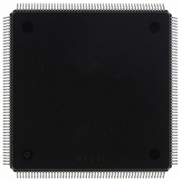
MCF5407AI220 Freescale Semiconductor, MCF5407AI220 Datasheet - Page 127

MCF5407AI220
Manufacturer Part Number
MCF5407AI220
Description
IC MPU 32B 220MHZ COLDF 208-FQFP
Manufacturer
Freescale Semiconductor
Series
MCF540xr
Specifications of MCF5407AI220
Core Processor
Coldfire V4
Core Size
32-Bit
Speed
220MHz
Connectivity
EBI/EMI, I²C, UART/USART
Peripherals
DMA, WDT
Number Of I /o
16
Program Memory Type
ROMless
Ram Size
4K x 8
Voltage - Supply (vcc/vdd)
1.65 V ~ 3.6 V
Oscillator Type
External
Operating Temperature
0°C ~ 70°C
Package / Case
208-FQFP
Maximum Clock Frequency
220 MHz
Operating Supply Voltage
1.8 V, 3.3 V
Maximum Operating Temperature
+ 105 C
Mounting Style
SMD/SMT
Minimum Operating Temperature
0 C
Program Memory Size
24KB
Cpu Speed
220MHz
Embedded Interface Type
I2C, UART
Digital Ic Case Style
FQFP
No. Of Pins
208
Supply Voltage Range
3.3V
Rohs Compliant
Yes
For Use With
M5407C3 - KIT EVAL FOR MCF5407 W/ETHERNET
Lead Free Status / RoHS Status
Lead free / RoHS Compliant
Eeprom Size
-
Program Memory Size
-
Data Converters
-
Lead Free Status / Rohs Status
Lead free / RoHS Compliant
Available stocks
Company
Part Number
Manufacturer
Quantity
Price
Company:
Part Number:
MCF5407AI220
Manufacturer:
freescaie
Quantity:
6
Company:
Part Number:
MCF5407AI220
Manufacturer:
Freescale Semiconductor
Quantity:
135
Company:
Part Number:
MCF5407AI220
Manufacturer:
FREESCALE
Quantity:
1 831
Company:
Part Number:
MCF5407AI220
Manufacturer:
Freescale Semiconductor
Quantity:
10 000
- Current page: 127 of 546
- Download datasheet (7Mb)
Accesses are attempted in the following order:
4.4 SRAM Programming Model
The SRAM programming model consists of RAMBAR0 and RAMBAR1.
4.4.1 SRAM Base Address Registers (RAMBAR0/RAMBAR1)
The SRAM modules are configured through the RAMBARs, shown in Figure 4-1.
Address
RAMBARn fields are described in detail in Table 4-1.
31–11 BA
10–9
8
7
Reset
Bits
Field
R/W
1. SRAM
2. Cache (if space is defined as cacheable)
3. External access
• Each RAMBAR holds the base address of the SRAM. The MOVEC instruction
• Each RAMBAR can be read or written from the debug module in a similar manner.
• All undefined RAMBAR bits are reserved. These bits are ignored during writes to
• The valid bits, RAMBARn[V], are cleared at reset, disabling the SRAM modules.
provides write-only access to this register from the processor.
the RAMBAR and return zeros when read from the debug module.
All other bits are unaffected.
—
WP
D/I
31
Name
Base address. Defines the SRAM module’s word-aligned base address. Each SRAM module
occupies a 2-Kbyte space defined by the contents of BA. SRAM may reside on any 2-Kbyte
boundary in the 4-Gbyte address space.
Reserved, should be cleared.
Write protect. Controls read/write properties of the SRAM.
0 Allows read and write accesses to the SRAM module
1 Allows only read accesses to the SRAM module. Any attempted write reference generates an
Data/instruction bus. Indicates whether SRAM is connected to the internal data or instruction bus.
0 Data bus
1 Instruction bus
Figure 4-1. SRAM Base Address Registers (RAMBARn)
access error exception to the ColdFire processor core.
CPU space + 0xC04 (RAMBAR0), CPU space + 0xC05 (RAMBAR1)
Table 4-1. RAMBARn Field Description
BA
Chapter 4. Local Memory
W for CPU; R/W for debug
—
Description
11
10
—
9
WP D/I — C/I SC SD UC UD
8
7
SRAM Programming Model
6
5
4
3
2
1
4-3
V
0
0
Related parts for MCF5407AI220
Image
Part Number
Description
Manufacturer
Datasheet
Request
R
Part Number:
Description:
Mcf5407 Coldfire Integrated Microprocessor User
Manufacturer:
Freescale Semiconductor, Inc
Datasheet:
Part Number:
Description:
Manufacturer:
Freescale Semiconductor, Inc
Datasheet:
Part Number:
Description:
Manufacturer:
Freescale Semiconductor, Inc
Datasheet:
Part Number:
Description:
Manufacturer:
Freescale Semiconductor, Inc
Datasheet:
Part Number:
Description:
Manufacturer:
Freescale Semiconductor, Inc
Datasheet:
Part Number:
Description:
Manufacturer:
Freescale Semiconductor, Inc
Datasheet:
Part Number:
Description:
Manufacturer:
Freescale Semiconductor, Inc
Datasheet:
Part Number:
Description:
Manufacturer:
Freescale Semiconductor, Inc
Datasheet:
Part Number:
Description:
Manufacturer:
Freescale Semiconductor, Inc
Datasheet:
Part Number:
Description:
Manufacturer:
Freescale Semiconductor, Inc
Datasheet:
Part Number:
Description:
Manufacturer:
Freescale Semiconductor, Inc
Datasheet:
Part Number:
Description:
Manufacturer:
Freescale Semiconductor, Inc
Datasheet:
Part Number:
Description:
Manufacturer:
Freescale Semiconductor, Inc
Datasheet:
Part Number:
Description:
Manufacturer:
Freescale Semiconductor, Inc
Datasheet:
Part Number:
Description:
Manufacturer:
Freescale Semiconductor, Inc
Datasheet:


