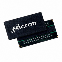
MT47H64M8CB-3:B Micron Technology Inc, MT47H64M8CB-3:B Datasheet - Page 26

MT47H64M8CB-3:B
Manufacturer Part Number
MT47H64M8CB-3:B
Description
IC DDR2 SDRAM 512MBIT 3NS 60FBGA
Manufacturer
Micron Technology Inc
Datasheet
1.MT47H64M8CB-5EB.pdf
(133 pages)
Specifications of MT47H64M8CB-3:B
Format - Memory
RAM
Memory Type
DDR2 SDRAM
Memory Size
512M (64M x 8)
Speed
3ns
Interface
Parallel
Voltage - Supply
1.7 V ~ 1.9 V
Operating Temperature
0°C ~ 85°C
Package / Case
60-FBGA
Lead Free Status / RoHS Status
Lead free / RoHS Compliant
Available stocks
Company
Part Number
Manufacturer
Quantity
Price
Company:
Part Number:
MT47H64M8CB-3:B
Manufacturer:
MICRON
Quantity:
12 388
Company:
Part Number:
MT47H64M8CB-3:B
Manufacturer:
Micron Technology Inc
Quantity:
10 000
Company:
Part Number:
MT47H64M8CB-3:B TR
Manufacturer:
Micron Technology Inc
Quantity:
10 000
Off-Chip Driver (OCD) Impedance Calibration
Posted CAS Additive Latency (AL)
Figure 11:
PDF: 09005aef8117c18e, Source: 09005aef8211b2e6
512MbDDR2_2.fm - Rev. K 8/06 EN
COMMAND
DQS, DQS#
CK#
DQ
CK
ACTIVE n
T0
READ Latency
Notes:
READ n
T1
which point the ODT ball will determine the R
the ODT function, ODT may not be driven HIGH until eight clocks after the EMR has
been enabled. See “ODT Timing” on page 74 for ODT timing diagrams.
The OFF-CHIP DRIVER function is no longer supported and must be set to the default
state. See “Initialization” on page 16 for proper setting of OCD defaults.
Posted CAS additive latency (AL) is supported to make the command and data bus effi-
cient for sustainable bandwidths in DDR2 SDRAM. Bits E3–E5 define the value of AL, as
shown in Figure 10 on page 24. Bits E3–E5 allow the user to program the DDR2 SDRAM
with an inverse AL of 0, 1, 2, 3, or 4 clocks. Reserved states should not be used as
unknown operation or incompatibility with future versions may result.
In this operation, the DDR2 SDRAM allows a READ or WRITE command to be issued
prior to
using this feature would set AL =
held for the time of the AL before it is issued internally to the DDR2 SDRAM device. RL is
controlled by the sum of AL and CL; RL = AL + CL. Write latency (WL) is equal to RL
minus one clock; WL = AL + CL - 1 x
example of a WL is shown in Figure 12 on page 27.
1. BL = 4.
2. Shown with nominal
3. CL = 3.
4. AL = 2.
5. RL = AL +CL = 5.
t RCD (MIN)
t
AL = 2
RCD (MIN) with the requirement that AL ≤
NOP
T2
NOP
T3
t
AC,
RL = 5
t
DQSCK, and
Off-Chip Driver (OCD) Impedance Calibration
26
NOP
t
T4
RCD (MIN) - 1 x
t
CK. An example of RL is shown in Figure 11. An
CL = 3
Micron Technology, Inc., reserves the right to change products or specifications without notice.
t
DQSQ.
NOP
T5
512Mb: x4, x8, x16 DDR2 SDRAM
TT
(EFF) value. Any time the EMR enables
t
CK. The READ or WRITE command is
t
RCD (MIN). A typical application
NOP
T6
D
OUT
n
TRANSITIONING DATA
©2004 Micron Technology, Inc. All rights reserved.
D
n + 1
OUT
NOP
T7
D
n + 2
OUT
D
n + 3
OUT
DON’T CARE
NOP
T8


