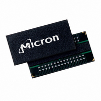
MT47H64M8CB-3:B Micron Technology Inc, MT47H64M8CB-3:B Datasheet - Page 19

MT47H64M8CB-3:B
Manufacturer Part Number
MT47H64M8CB-3:B
Description
IC DDR2 SDRAM 512MBIT 3NS 60FBGA
Manufacturer
Micron Technology Inc
Datasheet
1.MT47H64M8CB-5EB.pdf
(133 pages)
Specifications of MT47H64M8CB-3:B
Format - Memory
RAM
Memory Type
DDR2 SDRAM
Memory Size
512M (64M x 8)
Speed
3ns
Interface
Parallel
Voltage - Supply
1.7 V ~ 1.9 V
Operating Temperature
0°C ~ 85°C
Package / Case
60-FBGA
Lead Free Status / RoHS Status
Lead free / RoHS Compliant
Available stocks
Company
Part Number
Manufacturer
Quantity
Price
Company:
Part Number:
MT47H64M8CB-3:B
Manufacturer:
MICRON
Quantity:
12 388
Company:
Part Number:
MT47H64M8CB-3:B
Manufacturer:
Micron Technology Inc
Quantity:
10 000
Company:
Part Number:
MT47H64M8CB-3:B TR
Manufacturer:
Micron Technology Inc
Quantity:
10 000
Mode Register (MR)
Burst Length
PDF: 09005aef8117c18e, Source: 09005aef8211b2e6
512MbDDR2_2.fm - Rev. K 8/06 EN
The mode register is used to define the specific mode of operation of the DDR2 SDRAM.
This definition includes the selection of a burst length, burst type, CAS latency, oper-
ating mode, DLL RESET, write recovery, and power-down mode, as shown in Figure 8 on
page 20. Contents of the mode register can be altered by re-executing the LOAD MODE
(LM) command. If the user chooses to modify only a subset of the MR variables, all vari-
ables (M0–M13 for x4 and x8 or M0–M12 for x16) must be programmed when the
command is issued.
The MR is programmed via the LM command (bits BA1–BA0 = 0, 0) and other bits (M13–
M0 for x4 and x8, M12–M0 for x16) will retain the stored information until it is
programmed again or the device loses power (except for bit M8, which is self-clearing).
Reprogramming the mode register will not alter the contents of the memory array,
provided it is performed correctly.
The LM command can only be issued (or reissued) when all banks are in the precharged
state (idle state) and no bursts are in progress. The controller must wait the specified
time
Violating either of these requirements will result in unspecified operation.
Burst length is defined by bits M0–M3, as shown in Figure 8 on page 20. Read and write
accesses to the DDR2 SDRAM are burst-oriented, with the burst length being program-
mable to either four or eight. The burst length determines the maximum number of
column locations that can be accessed for a given READ or WRITE command.
When a READ or WRITE command is issued, a block of columns equal to the burst
length is effectively selected. All accesses for that burst take place within this block,
meaning that the burst will wrap within the block if a boundary is reached. The block is
uniquely selected by A2–Ai when BL = 4 and by A3–Ai when BL = 8 (where Ai is the most
significant column address bit for a given configuration). The remaining (least signifi-
cant) address bit(s) is (are) used to select the starting location within the block. The
programmed burst length applies to both READ and WRITE bursts.
t
MRD before initiating any subsequent operations such as an ACTIVE command.
19
Micron Technology, Inc., reserves the right to change products or specifications without notice.
512Mb: x4, x8, x16 DDR2 SDRAM
Mode Register (MR)
©2004 Micron Technology, Inc. All rights reserved.


