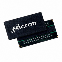
MT47H64M8CB-3:B Micron Technology Inc, MT47H64M8CB-3:B Datasheet - Page 17

MT47H64M8CB-3:B
Manufacturer Part Number
MT47H64M8CB-3:B
Description
IC DDR2 SDRAM 512MBIT 3NS 60FBGA
Manufacturer
Micron Technology Inc
Datasheet
1.MT47H64M8CB-5EB.pdf
(133 pages)
Specifications of MT47H64M8CB-3:B
Format - Memory
RAM
Memory Type
DDR2 SDRAM
Memory Size
512M (64M x 8)
Speed
3ns
Interface
Parallel
Voltage - Supply
1.7 V ~ 1.9 V
Operating Temperature
0°C ~ 85°C
Package / Case
60-FBGA
Lead Free Status / RoHS Status
Lead free / RoHS Compliant
Available stocks
Company
Part Number
Manufacturer
Quantity
Price
Company:
Part Number:
MT47H64M8CB-3:B
Manufacturer:
MICRON
Quantity:
12 388
Company:
Part Number:
MT47H64M8CB-3:B
Manufacturer:
Micron Technology Inc
Quantity:
10 000
Company:
Part Number:
MT47H64M8CB-3:B TR
Manufacturer:
Micron Technology Inc
Quantity:
10 000
PDF: 09005aef8117c18e, Source: 09005aef8211b2e6
512MbDDR2_2.fm - Rev. K 8/06 EN
Notes:
10. Issue a LOAD MODE command for DLL RESET. 200 cycles of clock input is required to lock
11. Issue PRECHARGE ALL command.
12. Issue two or more REFRESH commands.
1. Applying power; if CKE is maintained below 0.2 x V
2. CKE uses LVCMOS input levels prior to state T0 to ensure DQs are High-Z during device
3. PRE = PRECHARGE command, LM = LOAD MODE command, MR = Mode Register, EMR =
4. DM represents DM for x4, x8 configurations and UDM, LDM for x16 configuration; DQS rep-
5. For a minimum of 200µs after stable power and clock (CK, CK#), apply NOP or DESELECT
6. Wait a minimum of 400ns, then issue a PRECHARGE ALL command.
7. Issue a LOAD MODE command to the EMR(2). (To issue an EMR(2) command, provide LOW
8. Issue a LOAD MODE command to the EMR(3). (To issue an EMR(3) command, provide HIGH
9. Issue a LOAD MODE command to the EMR to enable DLL. To issue a DLL ENABLE command,
tee R
ODT ball (all other inputs may be undefined; I/Os and outputs must be less than V
ing voltage ramp time to avoid DDR2 SDRAM device latch-up). V
the device; however,
ing two sets of conditions (A or B) must be met to obtain a stable supply state (stable supply
defined as V
ues as stated in Table 20 on page 84):
power-up prior to V
levels. Once CKE transitions to a high level, it must stay HIGH for the duration of the initial-
ization sequence.
extended mode register, EMR2 = extended mode register 2, EMR3 = extended mode regis-
ter 3, REF = REFRESH command, ACT = ACTIVE command, A10 = PRECHARGE ALL, CODE =
desired values for mode registers (bank addresses are required to be decoded), VALID - any
valid command/address, RA = row address, bank address.
resents DQS, DQS#, UDQS, UDQS#, LDQS, LDQS#, RDQS, RDQS# for the appropriate configu-
ration (x4, x8, x16); DQ represents DQ0–DQ3 for x4, DQ–DQ7 for x8, and DQ0–DQ15 for x16.
commands, then take CKE HIGH.
to BA0, and provide HIGH to BA1.) Set register E7 to “0” or “1;” all others must be “0.”
to BA0 and BA1.) Set all registers to “0.”
provide LOW to BA1 and A0; provide HIGH to BA0. Bits E7, E8, and E9 can be set to “0” or
“1;” Micron recommends setting them to “0.”
the DLL. (To issue a DLL RESET, provide HIGH to A8 and provide LOW to BA1 and BA0.) CKE
must be HIGH the entire time.
longer than 200ms; during the V
ramping is complete (when V
age ramping, for both AC and DC levels, until supply voltage ramping completes (V
crosses V
A.
B.
TT
Single power source: The V
• V
• V
• V
• V
Multiple power sources: V
• Apply V
• Apply V
• V
• Apply V
(ODT resistance) is off, V
ply ramp time
time must be ≤200ms from when V
when V
V
supply ramp time; V
V
DD
TT
DD
TT
REF
DD
DD
REF
(MIN) is achieved must be no greater than 500ms
DD
, V
is limited to 0.95V MAX
Q ≥ V
is ramping, current can be supplied from V
[MIN]). Once supply voltage ramping is complete, Table 20 specifications apply.
tracks V
must track V
, V
DD
DD
DD
DD
TT
DD
L, and V
REF
; the V
(MIN) is achieved to when V
Q before or at the same time as V
and V
L, V
REF
t
DD
at all times
V
TT
being stable. After state T0, CKE is required to have SSTL_18 input
DD
Q/2; V
TT
DD
DD
should be ≥0 to avoid device latch-up. At least one of the follow-
DD
Q, V
voltage ramp time from when V
L before or at the same time as V
Q are driven from a single power converter output
Q/2; V
DD
17
REF
REF
DD
Q ≥ V
REF
DD
Q crosses V
, and V
must be within ±0.3V with respect to V
DD
DD
REF
must be valid and a low level must be applied to the
≥ V
REF
voltage ramp, |V
voltage ramp from 300mV to V
must be within ±0.3V with respect to V
Micron Technology, Inc., reserves the right to change products or specifications without notice.
DD
must be met at all times
TT
L ≥ V
are between their minimum and maximum val-
DD
DD
512Mb: x4, x8, x16 DDR2 SDRAM
DD
ramps from 300mV to V
DD
[MIN]), Table 20 specifications apply.
DD
Q must be maintained during supply volt-
Q (MIN) is achieved must be ≤500ms; while
Q, outputs remain disabled. To guaran-
TT
DD
; the V
DD
- V
DD
through the device to V
DD
Q| ≤ 0.3V. Once supply voltage
DD
DD
Q (MIN) is achieved to when
Q; V
Q voltage ramp time from
©2004 Micron Technology, Inc. All rights reserved.
TT
is not applied directly to
DD
DD
/V
DD
(MIN) must take no
DD
DD
(MIN)
Initialization
Q/2 during sup-
L voltage ramp
DD
Q/2 during
DD
DD
Q dur-
DD
Q
Q


