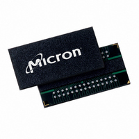
MT47H64M8CB-3:B Micron Technology Inc, MT47H64M8CB-3:B Datasheet - Page 126

MT47H64M8CB-3:B
Manufacturer Part Number
MT47H64M8CB-3:B
Description
IC DDR2 SDRAM 512MBIT 3NS 60FBGA
Manufacturer
Micron Technology Inc
Datasheet
1.MT47H64M8CB-5EB.pdf
(133 pages)
Specifications of MT47H64M8CB-3:B
Format - Memory
RAM
Memory Type
DDR2 SDRAM
Memory Size
512M (64M x 8)
Speed
3ns
Interface
Parallel
Voltage - Supply
1.7 V ~ 1.9 V
Operating Temperature
0°C ~ 85°C
Package / Case
60-FBGA
Lead Free Status / RoHS Status
Lead free / RoHS Compliant
Available stocks
Company
Part Number
Manufacturer
Quantity
Price
Company:
Part Number:
MT47H64M8CB-3:B
Manufacturer:
MICRON
Quantity:
12 388
Company:
Part Number:
MT47H64M8CB-3:B
Manufacturer:
Micron Technology Inc
Quantity:
10 000
Company:
Part Number:
MT47H64M8CB-3:B TR
Manufacturer:
Micron Technology Inc
Quantity:
10 000
Notes
PDF: 09005aef8117c18e, Source: 09005aef8211b2e6
512MbDDR2_2.fm - Rev. K 8/06 EN
10.
1. All voltages are referenced to V
2. Tests for AC timing, I
3. Outputs measured with equivalent load:
4. AC timing and I
5. The AC and DC input level specifications are as defined in the SSTL_18 standard (i.e.,
6. There are two sets of values listed for Command/Address:
7. The values listed are for the differential DQS strobe (DQS and DQS#) with a differen-
8.
9. This maximum value is derived from the referenced test load.
Output
(V
OUT
at nominal reference/supply voltage levels, but the related specifications and device
operation are guaranteed for the full voltage range specified. ODT is disabled for all
measurements that are not ODT-specific.
ment and parameter specifications are guaranteed for the specified AC input levels
under normal use conditions. The slew rate for the input signals used to test the
device is 1.0 V/ns for signals in the range between V
other than 1.0 V/ns may require the timing parameters to be derated as specified.
the receiver will effectively switch as a result of the signal crossing the AC input level
and will remain in that state as long as the signal does not ring back above [below] the
DC input LOW [HIGH] level).
t
at V
defined values, referenced from the logic trip points.
for a rising signal and V
for a rising signal and V
not equal to 1 V/ns, then the baseline values must be derated by adding the values
from Tables 26 and 27 on page 89.
tial slew rate of 2 V/ns (1 V/ns for each signal). There are two sets of values listed:
t
baseline values of
baseline values,
trip points.
signal, while
ing signal. If the differential DQS slew rate is not equal to 2 V/ns, then the baseline val-
ues must be derated by adding the values from Tables 28 and 29 on pages 94–95. If the
DQS differential strobe feature is not enabled, then the DQS strobe is single-ended,
the baseline values not applicable, and timing is not referenced to the logic trip
points. Single-ended DQS data timing is referenced to DQS crossing V
timing values for a single-ended DQS strobe are listed in Tables 30–33 on pages 96–97;
listed values are already derated for slew rate variations and can be used directly from
the table.
t
tions. These parameters are not referenced to a specific voltage level, but specify
when the device output is no longer driving (
over
t
IS
DH
HZ and
LZ (MIN) will prevail over a
a
)
V
,
REF
a
TT =
t
t
IH
DQSCK (MAX) +
and
when the slew rate is 1 V/ns. The baseline values,
a
V
t
values (for reference only) are equivalent to the baseline values of
LZ transitions occur in the same access time windows as valid data transi-
DD
t
25Ω
DS
Reference
Point
Q/2
t
DS
t
b
DH
,
b
t
DD
DH
t
is referenced from V
DS
b
t
is referenced from V
tests may use a V
DS
b
b
DD
. The
,
b
t
t
DH
,
RPST (MAX) condition.
IH
IL
, and electrical AC and DC characteristics may be conducted
t
DH
(
(
AC
DC
t
b
126
DS
, are the JEDEC-defined values, referenced from the logic
b
) for a falling signal, while
t
) for a falling signal. If the Command/Address slew rate is
DQSCK (MIN) +
a
at V
,
SS
t
DH
.
REF
a
IL
Micron Technology, Inc., reserves the right to change products or specifications without notice.
when the slew rate is 2 V/ns, differentially. The
IH
values (for reference only) are equivalent to the
-to-V
IL
(
AC
(
DC
) for a rising signal and V
512Mb: x4, x8, x16 DDR2 SDRAM
IH
) for a rising signal and V
t
swing of up to 1.0V in the test environ-
HZ) or begins driving (
t
RPRE (MAX) condition.
IL
t
(
IS
AC
t
IH
b
) and V
t
is referenced from V
b
IS
t
IS
is referenced from V
b
©2004 Micron Technology, Inc. All rights reserved.
a
,
,
t
t
IH
t
HZ (MAX) will prevail
IH
IH
b
(
a
, are the JEDEC-
AC
IL
and
t
(
). Slew rates
IH
LZ).
AC
REF
(
t
DC
) for a falling
IS
. The correct
b
) for a fall-
,
t
IS
t
IH
IH
b
Notes
,
b
(
IL
t
. The
AC
t
IH
DS
(
DC
)
b
a
)
,


