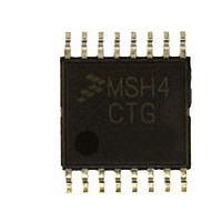
MC9S08SH4CTG Freescale, MC9S08SH4CTG Datasheet - Page 76

MC9S08SH4CTG
Manufacturer Part Number
MC9S08SH4CTG
Description
Manufacturer
Freescale
Datasheet
1.MC9S08SH4CTG.pdf
(338 pages)
Specifications of MC9S08SH4CTG
Cpu Family
HCS08
Device Core Size
8b
Frequency (max)
40MHz
Interface Type
I2C/SCI/SPI
Total Internal Ram Size
256Byte
# I/os (max)
13
Number Of Timers - General Purpose
1
Operating Supply Voltage (typ)
3.3/5V
Operating Supply Voltage (max)
5.5V
Operating Supply Voltage (min)
2.7V
On-chip Adc
8-chx10-bit
Instruction Set Architecture
CISC
Operating Temp Range
-40C to 85C
Operating Temperature Classification
Industrial
Mounting
Surface Mount
Pin Count
16
Package Type
TSSOP
Program Memory Type
Flash
Program Memory Size
4KB
Lead Free Status / RoHS Status
Compliant
Available stocks
Company
Part Number
Manufacturer
Quantity
Price
Company:
Part Number:
MC9S08SH4CTG
Manufacturer:
FREESCAL
Quantity:
96
Company:
Part Number:
MC9S08SH4CTG
Manufacturer:
Freescale
Quantity:
8 727
- Current page: 76 of 338
- Download datasheet (4Mb)
Chapter 6 Parallel Input/Output Control
It is a good programming practice to write to the port data register before changing the direction of a port
pin to become an output. This ensures that the pin will not be driven momentarily with an old data value
that happened to be in the port data register.
6.2
Associated with the parallel I/O ports is a set of registers located in the high page register space that operate
independently of the parallel I/O registers. These registers are used to control pull-ups, slew rate, and drive
strength for the pins.
An internal pull-up device can be enabled for each port pin by setting the corresponding bit in the pull-up
enable register (PTxPEn). The pull-up device is disabled if the pin is configured as an output by the parallel
I/O control logic or any shared peripheral function regardless of the state of the corresponding pull-up
enable register bit. The pull-up device is also disabled if the pin is controlled by an analog function.
Slew rate control can be enabled for each port pin by setting the corresponding bit in the slew rate control
register (PTxSEn). When enabled, slew control limits the rate at which an output can transition in order to
reduce EMC emissions. Slew rate control has no effect on pins that are configured as inputs.
An output pin can be selected to have high output drive strength by setting the corresponding bit in the
drive strength select register (PTxDSn). When high drive is selected, a pin is capable of sourcing and
sinking greater current. Even though every I/O pin can be selected as high drive, the user must ensure that
the total current source and sink limits for the MCU are not exceeded. Drive strength selection is intended
to affect the DC behavior of I/O pins. However, the AC behavior is also affected. High drive allows a pin
to drive a greater load with the same switching speed as a low drive enabled pin into a smaller load.
Because of this, the EMC emissions may be affected by enabling pins as high drive.
76
Pull-up, Slew Rate, and Drive Strength
Port Read
BUSCLK
Data
MC9S08SH8 MCU Series Data Sheet, Rev. 3
Figure 6-1. Parallel I/O Block Diagram
PTxDDn
D
D
PTxDn
Q
Q
1
0
Synchronizer
Output Enable
Output Data
Freescale Semiconductor
Input Data
Related parts for MC9S08SH4CTG
Image
Part Number
Description
Manufacturer
Datasheet
Request
R

Part Number:
Description:
TOWER ELEVATOR BOARDS HARDWARE
Manufacturer:
Freescale Semiconductor
Datasheet:

Part Number:
Description:
TOWER SERIAL I/O HARDWARE
Manufacturer:
Freescale Semiconductor
Datasheet:

Part Number:
Description:
LCD MODULE FOR TWR SYSTEM
Manufacturer:
Freescale Semiconductor
Datasheet:

Part Number:
Description:
DAUGHTER LCD WVGA I.MX51
Manufacturer:
Freescale Semiconductor
Datasheet:

Part Number:
Description:
TOWER SYSTEM BOARD MPC5125
Manufacturer:
Freescale Semiconductor
Datasheet:

Part Number:
Description:
KIT EVALUATION I.MX51
Manufacturer:
Freescale Semiconductor
Datasheet:

Part Number:
Description:
KIT DEVELOPMENT WINCE IMX25
Manufacturer:
Freescale Semiconductor
Datasheet:

Part Number:
Description:
TOWER SYSTEM KIT MPC5125
Manufacturer:
Freescale Semiconductor
Datasheet:

Part Number:
Description:
TOWER SYSTEM BOARD K40X256
Manufacturer:
Freescale Semiconductor
Datasheet:

Part Number:
Description:
TOWER SYSTEM KIT K40X256
Manufacturer:
Freescale Semiconductor
Datasheet:

Part Number:
Description:
Microcontrollers (MCU) MX28 PLATFORM DEV KIT
Manufacturer:
Freescale Semiconductor
Datasheet:

Part Number:
Description:
MCU, MPU & DSP Development Tools IAR KickStart Kit for Kinetis K60
Manufacturer:
Freescale Semiconductor
Datasheet:

Part Number:
Description:
24BIT HDMI MX535/08
Manufacturer:
Freescale Semiconductor
Datasheet:
Part Number:
Description:
Manufacturer:
Freescale Semiconductor, Inc
Datasheet:
Part Number:
Description:
Manufacturer:
Freescale Semiconductor, Inc
Datasheet:


