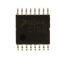
MC9S08SH4CTG Freescale, MC9S08SH4CTG Datasheet - Page 228

MC9S08SH4CTG
Manufacturer Part Number
MC9S08SH4CTG
Description
Manufacturer
Freescale
Datasheet
1.MC9S08SH4CTG.pdf
(338 pages)
Specifications of MC9S08SH4CTG
Cpu Family
HCS08
Device Core Size
8b
Frequency (max)
40MHz
Interface Type
I2C/SCI/SPI
Total Internal Ram Size
256Byte
# I/os (max)
13
Number Of Timers - General Purpose
1
Operating Supply Voltage (typ)
3.3/5V
Operating Supply Voltage (max)
5.5V
Operating Supply Voltage (min)
2.7V
On-chip Adc
8-chx10-bit
Instruction Set Architecture
CISC
Operating Temp Range
-40C to 85C
Operating Temperature Classification
Industrial
Mounting
Surface Mount
Pin Count
16
Package Type
TSSOP
Program Memory Type
Flash
Program Memory Size
4KB
Lead Free Status / RoHS Status
Compliant
Available stocks
Company
Part Number
Manufacturer
Quantity
Price
Company:
Part Number:
MC9S08SH4CTG
Manufacturer:
FREESCAL
Quantity:
96
Company:
Part Number:
MC9S08SH4CTG
Manufacturer:
Freescale
Quantity:
8 727
- Current page: 228 of 338
- Download datasheet (4Mb)
Chapter 15 Serial Peripheral Interface (S08SPIV3)
15.2
The SPI optionally shares four port pins. The function of these pins depends on the settings of SPI control
bits. When the SPI is disabled (SPE = 0), these four pins revert to being general-purpose port I/O pins that
are not controlled by the SPI.
15.2.1
When the SPI is enabled as a slave, this pin is the serial clock input. When the SPI is enabled as a master,
this pin is the serial clock output.
15.2.2
When the SPI is enabled as a master and SPI pin control zero (SPC0) is 0 (not bidirectional mode), this
pin is the serial data output. When the SPI is enabled as a slave and SPC0 = 0, this pin is the serial data
input. If SPC0 = 1 to select single-wire bidirectional mode, and master mode is selected, this pin becomes
the bidirectional data I/O pin (MOMI). Also, the bidirectional mode output enable bit determines whether
the pin acts as an input (BIDIROE = 0) or an output (BIDIROE = 1). If SPC0 = 1 and slave mode is
selected, this pin is not used by the SPI and reverts to being a general-purpose port I/O pin.
15.2.3
When the SPI is enabled as a master and SPI pin control zero (SPC0) is 0 (not bidirectional mode), this
pin is the serial data input. When the SPI is enabled as a slave and SPC0 = 0, this pin is the serial data
output. If SPC0 = 1 to select single-wire bidirectional mode, and slave mode is selected, this pin becomes
the bidirectional data I/O pin (SISO) and the bidirectional mode output enable bit determines whether the
pin acts as an input (BIDIROE = 0) or an output (BIDIROE = 1). If SPC0 = 1 and master mode is selected,
this pin is not used by the SPI and reverts to being a general-purpose port I/O pin.
15.2.4
When the SPI is enabled as a slave, this pin is the low-true slave select input. When the SPI is enabled as
a master and mode fault enable is off (MODFEN = 0), this pin is not used by the SPI and reverts to being
a general-purpose port I/O pin. When the SPI is enabled as a master and MODFEN = 1, the slave select
output enable bit determines whether this pin acts as the mode fault input (SSOE = 0) or as the slave select
output (SSOE = 1).
228
External Signal Description
SPSCK — SPI Serial Clock
MOSI — Master Data Out, Slave Data In
MISO — Master Data In, Slave Data Out
SS — Slave Select
BUS CLOCK
SPPR2:SPPR1:SPPR0
1, 2, 3, 4, 5, 6, 7, or 8
MC9S08SH8 MCU Series Data Sheet, Rev. 3
Figure 15-4. SPI Baud Rate Generation
PRESCALER
DIVIDE BY
2, 4, 8, 16, 32, 64, 128, or 256
CLOCK RATE DIVIDER
SPR2:SPR1:SPR0
DIVIDE BY
Freescale Semiconductor
MASTER
SPI
BIT RATE
Related parts for MC9S08SH4CTG
Image
Part Number
Description
Manufacturer
Datasheet
Request
R

Part Number:
Description:
TOWER ELEVATOR BOARDS HARDWARE
Manufacturer:
Freescale Semiconductor
Datasheet:

Part Number:
Description:
TOWER SERIAL I/O HARDWARE
Manufacturer:
Freescale Semiconductor
Datasheet:

Part Number:
Description:
LCD MODULE FOR TWR SYSTEM
Manufacturer:
Freescale Semiconductor
Datasheet:

Part Number:
Description:
DAUGHTER LCD WVGA I.MX51
Manufacturer:
Freescale Semiconductor
Datasheet:

Part Number:
Description:
TOWER SYSTEM BOARD MPC5125
Manufacturer:
Freescale Semiconductor
Datasheet:

Part Number:
Description:
KIT EVALUATION I.MX51
Manufacturer:
Freescale Semiconductor
Datasheet:

Part Number:
Description:
KIT DEVELOPMENT WINCE IMX25
Manufacturer:
Freescale Semiconductor
Datasheet:

Part Number:
Description:
TOWER SYSTEM KIT MPC5125
Manufacturer:
Freescale Semiconductor
Datasheet:

Part Number:
Description:
TOWER SYSTEM BOARD K40X256
Manufacturer:
Freescale Semiconductor
Datasheet:

Part Number:
Description:
TOWER SYSTEM KIT K40X256
Manufacturer:
Freescale Semiconductor
Datasheet:

Part Number:
Description:
Microcontrollers (MCU) MX28 PLATFORM DEV KIT
Manufacturer:
Freescale Semiconductor
Datasheet:

Part Number:
Description:
MCU, MPU & DSP Development Tools IAR KickStart Kit for Kinetis K60
Manufacturer:
Freescale Semiconductor
Datasheet:

Part Number:
Description:
24BIT HDMI MX535/08
Manufacturer:
Freescale Semiconductor
Datasheet:
Part Number:
Description:
Manufacturer:
Freescale Semiconductor, Inc
Datasheet:
Part Number:
Description:
Manufacturer:
Freescale Semiconductor, Inc
Datasheet:


