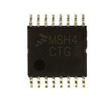
MC9S08SH4CTG Freescale, MC9S08SH4CTG Datasheet - Page 282

MC9S08SH4CTG
Manufacturer Part Number
MC9S08SH4CTG
Description
Manufacturer
Freescale
Datasheet
1.MC9S08SH4CTG.pdf
(338 pages)
Specifications of MC9S08SH4CTG
Cpu Family
HCS08
Device Core Size
8b
Frequency (max)
40MHz
Interface Type
I2C/SCI/SPI
Total Internal Ram Size
256Byte
# I/os (max)
13
Number Of Timers - General Purpose
1
Operating Supply Voltage (typ)
3.3/5V
Operating Supply Voltage (max)
5.5V
Operating Supply Voltage (min)
2.7V
On-chip Adc
8-chx10-bit
Instruction Set Architecture
CISC
Operating Temp Range
-40C to 85C
Operating Temperature Classification
Industrial
Mounting
Surface Mount
Pin Count
16
Package Type
TSSOP
Program Memory Type
Flash
Program Memory Size
4KB
Lead Free Status / RoHS Status
Compliant
Available stocks
Company
Part Number
Manufacturer
Quantity
Price
Company:
Part Number:
MC9S08SH4CTG
Manufacturer:
FREESCAL
Quantity:
96
Company:
Part Number:
MC9S08SH4CTG
Manufacturer:
Freescale
Quantity:
8 727
- Current page: 282 of 338
- Download datasheet (4Mb)
Active BDM:
Chapter 17 Development Support
17.4.1.1
This register can be read or written by serial BDC commands (READ_STATUS and WRITE_CONTROL)
but is not accessible to user programs because it is not located in the normal memory map of the MCU.
Reset in
282
Normal
Reset
BDMACT
BKPTEN
ENBDM
CLKSW
Field
FTS
W
7
6
5
4
3
R
ENBDM
Enable BDM (Permit Active Background Mode) — Typically, this bit is written to 1 by the debug host shortly
after the beginning of a debug session or whenever the debug host resets the target and remains 1 until a normal
reset clears it.
0 BDM cannot be made active (non-intrusive commands still allowed)
1 BDM can be made active to allow active background mode commands
Background Mode Active Status — This is a read-only status bit.
0 BDM not active (user application program running)
1 BDM active and waiting for serial commands
BDC Breakpoint Enable — If this bit is clear, the BDC breakpoint is disabled and the FTS (force tag select)
control bit and BDCBKPT match register are ignored.
0 BDC breakpoint disabled
1 BDC breakpoint enabled
Force/Tag Select — When FTS = 1, a breakpoint is requested whenever the CPU address bus matches the
BDCBKPT match register. When FTS = 0, a match between the CPU address bus and the BDCBKPT register
causes the fetched opcode to be tagged. If this tagged opcode ever reaches the end of the instruction queue,
the CPU enters active background mode rather than executing the tagged opcode.
0 Tag opcode at breakpoint address and enter active background mode if CPU attempts to execute that
1 Breakpoint match forces active background mode at next instruction boundary (address need not be an
Select Source for BDC Communications Clock — CLKSW defaults to 0, which selects the alternate BDC
clock source.
0 Alternate BDC clock source
1 MCU bus clock
0
1
7
BDC Status and Control Register (BDCSCR)
instruction
opcode)
= Unimplemented or Reserved
BDMACT
Figure 17-5. BDC Status and Control Register (BDCSCR)
0
1
6
Table 17-2. BDCSCR Register Field Descriptions
MC9S08SH8 MCU Series Data Sheet, Rev. 3
BKPTEN
0
0
5
FTS
0
0
4
Description
CLKSW
0
1
3
WS
0
0
2
Freescale Semiconductor
WSF
1
0
0
DVF
0
0
0
Related parts for MC9S08SH4CTG
Image
Part Number
Description
Manufacturer
Datasheet
Request
R

Part Number:
Description:
TOWER ELEVATOR BOARDS HARDWARE
Manufacturer:
Freescale Semiconductor
Datasheet:

Part Number:
Description:
TOWER SERIAL I/O HARDWARE
Manufacturer:
Freescale Semiconductor
Datasheet:

Part Number:
Description:
LCD MODULE FOR TWR SYSTEM
Manufacturer:
Freescale Semiconductor
Datasheet:

Part Number:
Description:
DAUGHTER LCD WVGA I.MX51
Manufacturer:
Freescale Semiconductor
Datasheet:

Part Number:
Description:
TOWER SYSTEM BOARD MPC5125
Manufacturer:
Freescale Semiconductor
Datasheet:

Part Number:
Description:
KIT EVALUATION I.MX51
Manufacturer:
Freescale Semiconductor
Datasheet:

Part Number:
Description:
KIT DEVELOPMENT WINCE IMX25
Manufacturer:
Freescale Semiconductor
Datasheet:

Part Number:
Description:
TOWER SYSTEM KIT MPC5125
Manufacturer:
Freescale Semiconductor
Datasheet:

Part Number:
Description:
TOWER SYSTEM BOARD K40X256
Manufacturer:
Freescale Semiconductor
Datasheet:

Part Number:
Description:
TOWER SYSTEM KIT K40X256
Manufacturer:
Freescale Semiconductor
Datasheet:

Part Number:
Description:
Microcontrollers (MCU) MX28 PLATFORM DEV KIT
Manufacturer:
Freescale Semiconductor
Datasheet:

Part Number:
Description:
MCU, MPU & DSP Development Tools IAR KickStart Kit for Kinetis K60
Manufacturer:
Freescale Semiconductor
Datasheet:

Part Number:
Description:
24BIT HDMI MX535/08
Manufacturer:
Freescale Semiconductor
Datasheet:
Part Number:
Description:
Manufacturer:
Freescale Semiconductor, Inc
Datasheet:
Part Number:
Description:
Manufacturer:
Freescale Semiconductor, Inc
Datasheet:


