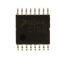
MC9S08SH4CTG Freescale, MC9S08SH4CTG Datasheet - Page 25

MC9S08SH4CTG
Manufacturer Part Number
MC9S08SH4CTG
Description
Manufacturer
Freescale
Datasheet
1.MC9S08SH4CTG.pdf
(338 pages)
Specifications of MC9S08SH4CTG
Cpu Family
HCS08
Device Core Size
8b
Frequency (max)
40MHz
Interface Type
I2C/SCI/SPI
Total Internal Ram Size
256Byte
# I/os (max)
13
Number Of Timers - General Purpose
1
Operating Supply Voltage (typ)
3.3/5V
Operating Supply Voltage (max)
5.5V
Operating Supply Voltage (min)
2.7V
On-chip Adc
8-chx10-bit
Instruction Set Architecture
CISC
Operating Temp Range
-40C to 85C
Operating Temperature Classification
Industrial
Mounting
Surface Mount
Pin Count
16
Package Type
TSSOP
Program Memory Type
Flash
Program Memory Size
4KB
Lead Free Status / RoHS Status
Compliant
Available stocks
Company
Part Number
Manufacturer
Quantity
Price
Company:
Part Number:
MC9S08SH4CTG
Manufacturer:
FREESCAL
Quantity:
96
Company:
Part Number:
MC9S08SH4CTG
Manufacturer:
Freescale
Quantity:
8 727
- Current page: 25 of 338
- Download datasheet (4Mb)
2.2.1
V
I/O buffer circuitry, ACMP and ADC modules, and to an internal voltage regulator. The internal voltage
regulator provides regulated lower-voltage source to the CPU and other internal circuitry of the MCU.
Typically, application systems have two separate capacitors across the power pins. In this case, there
should be a bulk electrolytic capacitor, such as a 10-μF tantalum capacitor, to provide bulk charge storage
for the overall system and a 0.1-μF ceramic bypass capacitor located as near to the MCU power pins as
practical to suppress high-frequency noise. Each pin must have a bypass capacitor for best noise
suppression.
Freescale Semiconductor
DD
V
DD
OPTIONAL
MANUAL
RESET
SYSTEM
POWER
and V
BACKGROUND HEADER
NOTES:
PTC0/TPM1CH0/ADP8
PTC1/TPM1CH1/ADP9
1. External crystal circuit not required if using the internal clock option.
2. RESET pin can only be used to reset into user mode, you can not enter BDM using RESET
3. RC filter on RESET pin recommended for noisy environments.
Power
SS
5 V
pin. BDM can be entered by holding MS low during POR or writing a 1 to BDFR in SBDFR
with MS low after issuing BDM command.
+
are the primary power supply pins for the MCU. This voltage source supplies power to all
PTC2/ADP10
PTC3/ADP11
10 μF
C
BLK
+
V
DD
C
0.1 μF
BY
4.7 kΩ–10 kΩ
0.1 μF
MC9S08SH8 MCU Series Data Sheet, Rev. 3
Figure 2-5. Basic System Connections
V
V
PORT
SS
DD
C
RESET
BKGD/MS
MC9S08SH8
PORT
PORT
A
B
C1
PTA0/PIA0/TPM1CH0/ADP0/ACMP+
PTA1/PIA1/TPM2CH0/ADP1/ACMP-
PTA2/PIA2/SDA/ADP2
PTA3/PIA3/SCL/ADP3
PTA4/ACMPO/BKGD/MS
PTA5/IRQ/TCLK/RESET
PTB0/PIB0/RxD/ADP4
PTB1/PIB1/TxD/ADP5
PTB2/PIB2/SPSCK/ADP6
PTB3/PIB3/MOSI/ADP7
PTB4/TPM2CH1/MISO
PTB5/TPM1CH1/SS
PTB6/SDA/XTAL
PTB7/SCL/EXTAL
X1
Chapter 2 Pins and Connections
R
F
NOTE 1
C2
R
S
25
Related parts for MC9S08SH4CTG
Image
Part Number
Description
Manufacturer
Datasheet
Request
R

Part Number:
Description:
TOWER ELEVATOR BOARDS HARDWARE
Manufacturer:
Freescale Semiconductor
Datasheet:

Part Number:
Description:
TOWER SERIAL I/O HARDWARE
Manufacturer:
Freescale Semiconductor
Datasheet:

Part Number:
Description:
LCD MODULE FOR TWR SYSTEM
Manufacturer:
Freescale Semiconductor
Datasheet:

Part Number:
Description:
DAUGHTER LCD WVGA I.MX51
Manufacturer:
Freescale Semiconductor
Datasheet:

Part Number:
Description:
TOWER SYSTEM BOARD MPC5125
Manufacturer:
Freescale Semiconductor
Datasheet:

Part Number:
Description:
KIT EVALUATION I.MX51
Manufacturer:
Freescale Semiconductor
Datasheet:

Part Number:
Description:
KIT DEVELOPMENT WINCE IMX25
Manufacturer:
Freescale Semiconductor
Datasheet:

Part Number:
Description:
TOWER SYSTEM KIT MPC5125
Manufacturer:
Freescale Semiconductor
Datasheet:

Part Number:
Description:
TOWER SYSTEM BOARD K40X256
Manufacturer:
Freescale Semiconductor
Datasheet:

Part Number:
Description:
TOWER SYSTEM KIT K40X256
Manufacturer:
Freescale Semiconductor
Datasheet:

Part Number:
Description:
Microcontrollers (MCU) MX28 PLATFORM DEV KIT
Manufacturer:
Freescale Semiconductor
Datasheet:

Part Number:
Description:
MCU, MPU & DSP Development Tools IAR KickStart Kit for Kinetis K60
Manufacturer:
Freescale Semiconductor
Datasheet:

Part Number:
Description:
24BIT HDMI MX535/08
Manufacturer:
Freescale Semiconductor
Datasheet:
Part Number:
Description:
Manufacturer:
Freescale Semiconductor, Inc
Datasheet:
Part Number:
Description:
Manufacturer:
Freescale Semiconductor, Inc
Datasheet:


