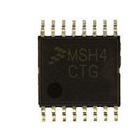
MC9S08SH4CTG Freescale, MC9S08SH4CTG Datasheet - Page 157

MC9S08SH4CTG
Manufacturer Part Number
MC9S08SH4CTG
Description
Manufacturer
Freescale
Datasheet
1.MC9S08SH4CTG.pdf
(338 pages)
Specifications of MC9S08SH4CTG
Cpu Family
HCS08
Device Core Size
8b
Frequency (max)
40MHz
Interface Type
I2C/SCI/SPI
Total Internal Ram Size
256Byte
# I/os (max)
13
Number Of Timers - General Purpose
1
Operating Supply Voltage (typ)
3.3/5V
Operating Supply Voltage (max)
5.5V
Operating Supply Voltage (min)
2.7V
On-chip Adc
8-chx10-bit
Instruction Set Architecture
CISC
Operating Temp Range
-40C to 85C
Operating Temperature Classification
Industrial
Mounting
Surface Mount
Pin Count
16
Package Type
TSSOP
Program Memory Type
Flash
Program Memory Size
4KB
Lead Free Status / RoHS Status
Compliant
Available stocks
Company
Part Number
Manufacturer
Quantity
Price
Company:
Part Number:
MC9S08SH4CTG
Manufacturer:
FREESCAL
Quantity:
96
Company:
Part Number:
MC9S08SH4CTG
Manufacturer:
Freescale
Quantity:
8 727
- Current page: 157 of 338
- Download datasheet (4Mb)
10.4
10.4.1
The seven states of the ICS are shown as a state diagram and are described below. The arrows indicate the
allowed movements between the states.
10.4.1.1
FLL engaged internal (FEI) is the default mode of operation and is entered when all the following
conditions occur:
Freescale Semiconductor
FLL Bypassed
External Low
Power(FBELP)
Field
IREFS=0
CLKS=10
BDM Disabled
and LP=1
1
0
Functional Description
Operational Modes
OSC Initialization — If the external reference clock is selected by ERCLKEN or by the ICS being in FEE, FBE,
or FBELP mode, and if EREFS is set, then this bit is set after the initialization cycles of the external oscillator
clock have completed. This bit is only cleared when either ERCLKEN or EREFS are cleared.
ICS Fine Trim — The FTRIM bit controls the smallest adjustment of the internal reference clock frequency.
Setting FTRIM will increase the period and clearing FTRIM will decrease the period by the smallest amount
possible.
FLL Engaged Internal (FEI)
Entered from any state
when MCU enters stop
Table 10-5. ICS Status and Control Register Field Descriptions (continued)
IREFS=0
CLKS=10
BDM Enabled
or LP =0
FLL Bypassed
External (FBE)
MC9S08SH8 MCU Series Data Sheet, Rev. 3
Figure 10-7. Clock Switching Modes
FLL Engaged
External (FEE)
FLL Engaged
Internal (FEI)
IREFS=1
CLKS=00
IREFS=0
CLKS=00
Stop
Description
Chapter 10 Internal Clock Source (S08ICSV2)
FLL Bypassed
Internal (FBI)
Returns to state that was active
before MCU entered stop, unless
RESET occurs while in stop.
IREFS=1
CLKS=01
BDM Enabled
or LP=0
FLL Bypassed
Internal Low
Power(FBILP)
IREFS=1
CLKS=01
BDM Disabled
and LP=1
157
Related parts for MC9S08SH4CTG
Image
Part Number
Description
Manufacturer
Datasheet
Request
R

Part Number:
Description:
TOWER ELEVATOR BOARDS HARDWARE
Manufacturer:
Freescale Semiconductor
Datasheet:

Part Number:
Description:
TOWER SERIAL I/O HARDWARE
Manufacturer:
Freescale Semiconductor
Datasheet:

Part Number:
Description:
LCD MODULE FOR TWR SYSTEM
Manufacturer:
Freescale Semiconductor
Datasheet:

Part Number:
Description:
DAUGHTER LCD WVGA I.MX51
Manufacturer:
Freescale Semiconductor
Datasheet:

Part Number:
Description:
TOWER SYSTEM BOARD MPC5125
Manufacturer:
Freescale Semiconductor
Datasheet:

Part Number:
Description:
KIT EVALUATION I.MX51
Manufacturer:
Freescale Semiconductor
Datasheet:

Part Number:
Description:
KIT DEVELOPMENT WINCE IMX25
Manufacturer:
Freescale Semiconductor
Datasheet:

Part Number:
Description:
TOWER SYSTEM KIT MPC5125
Manufacturer:
Freescale Semiconductor
Datasheet:

Part Number:
Description:
TOWER SYSTEM BOARD K40X256
Manufacturer:
Freescale Semiconductor
Datasheet:

Part Number:
Description:
TOWER SYSTEM KIT K40X256
Manufacturer:
Freescale Semiconductor
Datasheet:

Part Number:
Description:
Microcontrollers (MCU) MX28 PLATFORM DEV KIT
Manufacturer:
Freescale Semiconductor
Datasheet:

Part Number:
Description:
MCU, MPU & DSP Development Tools IAR KickStart Kit for Kinetis K60
Manufacturer:
Freescale Semiconductor
Datasheet:

Part Number:
Description:
24BIT HDMI MX535/08
Manufacturer:
Freescale Semiconductor
Datasheet:
Part Number:
Description:
Manufacturer:
Freescale Semiconductor, Inc
Datasheet:
Part Number:
Description:
Manufacturer:
Freescale Semiconductor, Inc
Datasheet:


