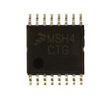
MC9S08SH4CTG Freescale, MC9S08SH4CTG Datasheet - Page 51

MC9S08SH4CTG
Manufacturer Part Number
MC9S08SH4CTG
Description
Manufacturer
Freescale
Datasheet
1.MC9S08SH4CTG.pdf
(338 pages)
Specifications of MC9S08SH4CTG
Cpu Family
HCS08
Device Core Size
8b
Frequency (max)
40MHz
Interface Type
I2C/SCI/SPI
Total Internal Ram Size
256Byte
# I/os (max)
13
Number Of Timers - General Purpose
1
Operating Supply Voltage (typ)
3.3/5V
Operating Supply Voltage (max)
5.5V
Operating Supply Voltage (min)
2.7V
On-chip Adc
8-chx10-bit
Instruction Set Architecture
CISC
Operating Temp Range
-40C to 85C
Operating Temperature Classification
Industrial
Mounting
Surface Mount
Pin Count
16
Package Type
TSSOP
Program Memory Type
Flash
Program Memory Size
4KB
Lead Free Status / RoHS Status
Compliant
Available stocks
Company
Part Number
Manufacturer
Quantity
Price
Company:
Part Number:
MC9S08SH4CTG
Manufacturer:
FREESCAL
Quantity:
96
Company:
Part Number:
MC9S08SH4CTG
Manufacturer:
Freescale
Quantity:
8 727
- Current page: 51 of 338
- Download datasheet (4Mb)
4.5.5
An access error occurs whenever the command execution protocol is violated.
Any of the following specific actions will cause the access error flag (FACCERR) in FSTAT to be set.
FACCERR must be cleared by writing a 1 to FACCERR in FSTAT before any command can be processed.
4.5.6
The block protection feature prevents the protected region of FLASH from program or erase changes.
Block protection is controlled through the FLASH protection register (FPROT). When enabled, block
protection begins at any 512 byte boundary below the last address of FLASH, 0xFFFF. (See
“FLASH Protection Register (FPROT and
After exit from reset, FPROT is loaded with the contents of the NVPROT location, which is in the
nonvolatile register block of the FLASH memory. FPROT cannot be changed directly from application
software so a runaway program cannot alter the block protection settings. Because NVPROT is within the
last 512 bytes of FLASH, if any amount of memory is protected, NVPROT is itself protected and cannot
be altered (intentionally or unintentionally) by the application software. FPROT can be written through
background debug commands, which allows a way to erase and reprogram a protected FLASH memory.
The block protection mechanism is illustrated in
last address of unprotected memory. This address is formed by concatenating FPS7:FPS1 with logic 1 bits
as shown. For example, to protect the last 1536 bytes of memory (addresses 0xFA00 through 0xFFFF), the
FPS bits must be set to 1111 100, which results in the value 0xF9FF as the last address of unprotected
memory. In addition to programming the FPS bits to the appropriate value, FPDIS (bit 0 of NVPROT) must
Freescale Semiconductor
•
•
•
•
•
•
•
•
•
•
Writing to a FLASH address before the internal FLASH clock frequency has been set by writing
to the FCDIV register
Writing to a FLASH address while FCBEF is not set (A new command cannot be started until the
command buffer is empty.)
Writing a second time to a FLASH address before launching the previous command (There is only
one write to FLASH for every command.)
Writing a second time to FCMD before launching the previous command (There is only one write
to FCMD for every command.)
Writing to any FLASH control register other than FCMD after writing to a FLASH address
Writing any command code other than the five allowed codes (0x05, 0x20, 0x25, 0x40, or 0x41)
to FCMD
Writing any FLASH control register other than the write to FSTAT (to clear FCBEF and launch the
command) after writing the command to FCMD
The MCU enters stop mode while a program or erase command is in progress (The command is
aborted.)
Writing the byte program, burst program, or page erase command code (0x20, 0x25, or 0x40) with
a background debug command while the MCU is secured (The background debug controller can
only do blank check and mass erase commands when the MCU is secure.)
Writing 0 to FCBEF to cancel a partial command
Access Errors
FLASH Block Protection
MC9S08SH8 MCU Series Data Sheet, Rev. 3
NVPROT)”).
Figure
4-4. The FPS bits are used as the upper bits of the
Chapter 4 Memory
Section 4.7.4,
51
Related parts for MC9S08SH4CTG
Image
Part Number
Description
Manufacturer
Datasheet
Request
R

Part Number:
Description:
TOWER ELEVATOR BOARDS HARDWARE
Manufacturer:
Freescale Semiconductor
Datasheet:

Part Number:
Description:
TOWER SERIAL I/O HARDWARE
Manufacturer:
Freescale Semiconductor
Datasheet:

Part Number:
Description:
LCD MODULE FOR TWR SYSTEM
Manufacturer:
Freescale Semiconductor
Datasheet:

Part Number:
Description:
DAUGHTER LCD WVGA I.MX51
Manufacturer:
Freescale Semiconductor
Datasheet:

Part Number:
Description:
TOWER SYSTEM BOARD MPC5125
Manufacturer:
Freescale Semiconductor
Datasheet:

Part Number:
Description:
KIT EVALUATION I.MX51
Manufacturer:
Freescale Semiconductor
Datasheet:

Part Number:
Description:
KIT DEVELOPMENT WINCE IMX25
Manufacturer:
Freescale Semiconductor
Datasheet:

Part Number:
Description:
TOWER SYSTEM KIT MPC5125
Manufacturer:
Freescale Semiconductor
Datasheet:

Part Number:
Description:
TOWER SYSTEM BOARD K40X256
Manufacturer:
Freescale Semiconductor
Datasheet:

Part Number:
Description:
TOWER SYSTEM KIT K40X256
Manufacturer:
Freescale Semiconductor
Datasheet:

Part Number:
Description:
Microcontrollers (MCU) MX28 PLATFORM DEV KIT
Manufacturer:
Freescale Semiconductor
Datasheet:

Part Number:
Description:
MCU, MPU & DSP Development Tools IAR KickStart Kit for Kinetis K60
Manufacturer:
Freescale Semiconductor
Datasheet:

Part Number:
Description:
24BIT HDMI MX535/08
Manufacturer:
Freescale Semiconductor
Datasheet:
Part Number:
Description:
Manufacturer:
Freescale Semiconductor, Inc
Datasheet:
Part Number:
Description:
Manufacturer:
Freescale Semiconductor, Inc
Datasheet:


