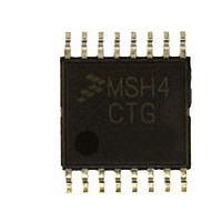
MC9S08SH4CTG Freescale, MC9S08SH4CTG Datasheet - Page 244

MC9S08SH4CTG
Manufacturer Part Number
MC9S08SH4CTG
Description
Manufacturer
Freescale
Datasheet
1.MC9S08SH4CTG.pdf
(338 pages)
Specifications of MC9S08SH4CTG
Cpu Family
HCS08
Device Core Size
8b
Frequency (max)
40MHz
Interface Type
I2C/SCI/SPI
Total Internal Ram Size
256Byte
# I/os (max)
13
Number Of Timers - General Purpose
1
Operating Supply Voltage (typ)
3.3/5V
Operating Supply Voltage (max)
5.5V
Operating Supply Voltage (min)
2.7V
On-chip Adc
8-chx10-bit
Instruction Set Architecture
CISC
Operating Temp Range
-40C to 85C
Operating Temperature Classification
Industrial
Mounting
Surface Mount
Pin Count
16
Package Type
TSSOP
Program Memory Type
Flash
Program Memory Size
4KB
Lead Free Status / RoHS Status
Compliant
Available stocks
Company
Part Number
Manufacturer
Quantity
Price
Company:
Part Number:
MC9S08SH4CTG
Manufacturer:
FREESCAL
Quantity:
96
Company:
Part Number:
MC9S08SH4CTG
Manufacturer:
Freescale
Quantity:
8 727
- Current page: 244 of 338
- Download datasheet (4Mb)
Chapter 16 Timer/PWM Module (S08TPMV3)
The TPM channels are programmable independently as input capture, output compare, or edge-aligned
PWM channels. Alternately, the TPM can be configured to produce CPWM outputs on all channels. When
the TPM is configured for CPWMs, the counter operates as an up/down counter; input capture, output
compare, and EPWM functions are not practical.
If a channel is configured as input capture, an internal pullup device may be enabled for that channel. The
details of how a module interacts with pin controls depends upon the chip implementation because the I/O
pins and associated general purpose I/O controls are not part of the module. Refer to the discussion of the
I/O port logic in a full-chip specification.
Because center-aligned PWMs are usually used to drive 3-phase AC-induction motors and brushless DC
motors, they are typically used in sets of three or six channels.
16.2
Table 16-2
one to eight. When an external clock is included, it can be shared with the same pin as any TPM channel;
however, it could be connected to a separate input pin. Refer to the I/O pin descriptions in full-chip
specification for the specific chip implementation.
Refer to documentation for the full-chip for details about reset states, port connections, and whether there
is any pullup device on these pins.
TPM channel pins can be associated with general purpose I/O pins and have passive pullup devices which
can be enabled with a control bit when the TPM or general purpose I/O controls have configured the
associated pin as an input. When no TPM function is enabled to use a corresponding pin, the pin reverts
to being controlled by general purpose I/O controls, including the port-data and data-direction registers.
Immediately after reset, no TPM functions are enabled, so all associated pins revert to general purpose I/O
control.
16.2.1
This section describes each user-accessible pin signal in detail. Although
pins together, any TPM pin can be shared with the external clock source signal. Since I/O pin logic is not
part of the TPM, refer to full-chip documentation for a specific derivative for more details about the
interaction of TPM pin functions and general purpose I/O controls including port data, data direction, and
pullup controls.
244
Signal Description
shows the user-accessible signals for the TPM. The number of channels may be varied from
1
2
Detailed Signal Descriptions
When preset, this signal can share any channel pin; however depending upon full-chip
implementation, this signal could be connected to a separate external pin.
n=channel number (1 to 8)
TPMxCHn
EXTCLK
Name
1
2
External clock source which may be selected to drive the TPM counter.
I/O pin associated with TPM channel n
MC9S08SH8 MCU Series Data Sheet, Rev. 3
Table 16-2. Signal Properties
Function
Table 16-2
Freescale Semiconductor
grouped all channel
Related parts for MC9S08SH4CTG
Image
Part Number
Description
Manufacturer
Datasheet
Request
R

Part Number:
Description:
TOWER ELEVATOR BOARDS HARDWARE
Manufacturer:
Freescale Semiconductor
Datasheet:

Part Number:
Description:
TOWER SERIAL I/O HARDWARE
Manufacturer:
Freescale Semiconductor
Datasheet:

Part Number:
Description:
LCD MODULE FOR TWR SYSTEM
Manufacturer:
Freescale Semiconductor
Datasheet:

Part Number:
Description:
DAUGHTER LCD WVGA I.MX51
Manufacturer:
Freescale Semiconductor
Datasheet:

Part Number:
Description:
TOWER SYSTEM BOARD MPC5125
Manufacturer:
Freescale Semiconductor
Datasheet:

Part Number:
Description:
KIT EVALUATION I.MX51
Manufacturer:
Freescale Semiconductor
Datasheet:

Part Number:
Description:
KIT DEVELOPMENT WINCE IMX25
Manufacturer:
Freescale Semiconductor
Datasheet:

Part Number:
Description:
TOWER SYSTEM KIT MPC5125
Manufacturer:
Freescale Semiconductor
Datasheet:

Part Number:
Description:
TOWER SYSTEM BOARD K40X256
Manufacturer:
Freescale Semiconductor
Datasheet:

Part Number:
Description:
TOWER SYSTEM KIT K40X256
Manufacturer:
Freescale Semiconductor
Datasheet:

Part Number:
Description:
Microcontrollers (MCU) MX28 PLATFORM DEV KIT
Manufacturer:
Freescale Semiconductor
Datasheet:

Part Number:
Description:
MCU, MPU & DSP Development Tools IAR KickStart Kit for Kinetis K60
Manufacturer:
Freescale Semiconductor
Datasheet:

Part Number:
Description:
24BIT HDMI MX535/08
Manufacturer:
Freescale Semiconductor
Datasheet:
Part Number:
Description:
Manufacturer:
Freescale Semiconductor, Inc
Datasheet:
Part Number:
Description:
Manufacturer:
Freescale Semiconductor, Inc
Datasheet:


