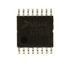
MC9S08SH4CTG Freescale, MC9S08SH4CTG Datasheet - Page 315

MC9S08SH4CTG
Manufacturer Part Number
MC9S08SH4CTG
Description
Manufacturer
Freescale
Datasheet
1.MC9S08SH4CTG.pdf
(338 pages)
Specifications of MC9S08SH4CTG
Cpu Family
HCS08
Device Core Size
8b
Frequency (max)
40MHz
Interface Type
I2C/SCI/SPI
Total Internal Ram Size
256Byte
# I/os (max)
13
Number Of Timers - General Purpose
1
Operating Supply Voltage (typ)
3.3/5V
Operating Supply Voltage (max)
5.5V
Operating Supply Voltage (min)
2.7V
On-chip Adc
8-chx10-bit
Instruction Set Architecture
CISC
Operating Temp Range
-40C to 85C
Operating Temperature Classification
Industrial
Mounting
Surface Mount
Pin Count
16
Package Type
TSSOP
Program Memory Type
Flash
Program Memory Size
4KB
Lead Free Status / RoHS Status
Compliant
Available stocks
Company
Part Number
Manufacturer
Quantity
Price
Company:
Part Number:
MC9S08SH4CTG
Manufacturer:
FREESCAL
Quantity:
96
Company:
Part Number:
MC9S08SH4CTG
Manufacturer:
Freescale
Quantity:
8 727
- Current page: 315 of 338
- Download datasheet (4Mb)
A.13 FLASH Specifications
This section provides details about program/erase times and program-erase endurance for the FLASH
memory.
Program and erase operations do not require any special power sources other than the normal V
For more detailed information about program/erase operations, see the Memory section.
Freescale Semiconductor
1
2
3
4
Num
These values are hardware state machine controlled. User code does not need to count cycles. This information supplied for
calculating approximate time to program and erase.
Typical endurance for FLASH is based on the intrinsic bit cell performance. For additional information on how Freescale
defines typical endurance, please refer to Engineering Bulletin EB619/D, Typical Endurance for Nonvolatile Memory.
Typical data retention values are based on intrinsic capability of the technology measured at high temperature and de-rated
to 25°C using the Arrhenius equation. For additional information on how Freescale defines typical data retention, please refer
to Engineering Bulletin EB618/D, Typical Data Retention for Nonvolatile Memory.
10
The frequency of this clock is controlled by a software setting.
1
2
3
5
6
7
8
9
4
—
—
—
—
—
—
—
—
C
C
C
Supply voltage for program/erase
Supply voltage for read operation
Internal FCLK frequency
Internal FCLK period (1/f
Byte program time (random location)
Byte program time (burst mode)
Page erase time
Mass erase time
Program/erase endurance
Data retention
T
T = 25°C
L
to T
H
= –40°C to +125°C
Characteristic
4
2
2
MC9S08SH8 MCU Series Data Sheet, Rev. 3
Table A-16. FLASH Characteristics
1
FCLK
3
)
2
2
V
Symbol
prog/erase
V
n
f
t
t
t
t
t
t
FCLK
Burst
Mass
D_ret
Page
Fcyc
prog
FLPE
Read
10,000
150
Min
2.7
2.7
15
—
5
100,000
Typical
20,000
4000
100
Appendix A Electrical Characteristics
—
9
4
6.67
Max
200
5.5
5.5
—
—
—
DD
cycles
years
supply.
t
t
t
t
Unit
kHz
Fcyc
Fcyc
Fcyc
Fcyc
μs
V
V
315
Related parts for MC9S08SH4CTG
Image
Part Number
Description
Manufacturer
Datasheet
Request
R

Part Number:
Description:
TOWER ELEVATOR BOARDS HARDWARE
Manufacturer:
Freescale Semiconductor
Datasheet:

Part Number:
Description:
TOWER SERIAL I/O HARDWARE
Manufacturer:
Freescale Semiconductor
Datasheet:

Part Number:
Description:
LCD MODULE FOR TWR SYSTEM
Manufacturer:
Freescale Semiconductor
Datasheet:

Part Number:
Description:
DAUGHTER LCD WVGA I.MX51
Manufacturer:
Freescale Semiconductor
Datasheet:

Part Number:
Description:
TOWER SYSTEM BOARD MPC5125
Manufacturer:
Freescale Semiconductor
Datasheet:

Part Number:
Description:
KIT EVALUATION I.MX51
Manufacturer:
Freescale Semiconductor
Datasheet:

Part Number:
Description:
KIT DEVELOPMENT WINCE IMX25
Manufacturer:
Freescale Semiconductor
Datasheet:

Part Number:
Description:
TOWER SYSTEM KIT MPC5125
Manufacturer:
Freescale Semiconductor
Datasheet:

Part Number:
Description:
TOWER SYSTEM BOARD K40X256
Manufacturer:
Freescale Semiconductor
Datasheet:

Part Number:
Description:
TOWER SYSTEM KIT K40X256
Manufacturer:
Freescale Semiconductor
Datasheet:

Part Number:
Description:
Microcontrollers (MCU) MX28 PLATFORM DEV KIT
Manufacturer:
Freescale Semiconductor
Datasheet:

Part Number:
Description:
MCU, MPU & DSP Development Tools IAR KickStart Kit for Kinetis K60
Manufacturer:
Freescale Semiconductor
Datasheet:

Part Number:
Description:
24BIT HDMI MX535/08
Manufacturer:
Freescale Semiconductor
Datasheet:
Part Number:
Description:
Manufacturer:
Freescale Semiconductor, Inc
Datasheet:
Part Number:
Description:
Manufacturer:
Freescale Semiconductor, Inc
Datasheet:


