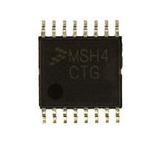
MC9S08SH4CTG Freescale, MC9S08SH4CTG Datasheet - Page 174

MC9S08SH4CTG
Manufacturer Part Number
MC9S08SH4CTG
Description
Manufacturer
Freescale
Datasheet
1.MC9S08SH4CTG.pdf
(338 pages)
Specifications of MC9S08SH4CTG
Cpu Family
HCS08
Device Core Size
8b
Frequency (max)
40MHz
Interface Type
I2C/SCI/SPI
Total Internal Ram Size
256Byte
# I/os (max)
13
Number Of Timers - General Purpose
1
Operating Supply Voltage (typ)
3.3/5V
Operating Supply Voltage (max)
5.5V
Operating Supply Voltage (min)
2.7V
On-chip Adc
8-chx10-bit
Instruction Set Architecture
CISC
Operating Temp Range
-40C to 85C
Operating Temperature Classification
Industrial
Mounting
Surface Mount
Pin Count
16
Package Type
TSSOP
Program Memory Type
Flash
Program Memory Size
4KB
Lead Free Status / RoHS Status
Compliant
Available stocks
Company
Part Number
Manufacturer
Quantity
Price
Company:
Part Number:
MC9S08SH4CTG
Manufacturer:
FREESCAL
Quantity:
96
Company:
Part Number:
MC9S08SH4CTG
Manufacturer:
Freescale
Quantity:
8 727
- Current page: 174 of 338
- Download datasheet (4Mb)
Chapter 11 Inter-Integrated Circuit (S08IICV2)
11.4.1.1
When the bus is free, no master device is engaging the bus (SCL and SDA lines are at logical high), a
master may initiate communication by sending a start signal. As shown in
defined as a high-to-low transition of SDA while SCL is high. This signal denotes the beginning of a new
data transfer (each data transfer may contain several bytes of data) and brings all slaves out of their idle
states.
11.4.1.2
The first byte of data transferred immediately after the start signal is the slave address transmitted by the
master. This is a seven-bit calling address followed by a R/W bit. The R/W bit tells the slave the desired
direction of data transfer.
Only the slave with a calling address that matches the one transmitted by the master responds by sending
back an acknowledge bit. This is done by pulling the SDA low at the ninth clock (see
No two slaves in the system may have the same address. If the IIC module is the master, it must not transmit
an address equal to its own slave address. The IIC cannot be master and slave at the same time. However,
if arbitration is lost during an address cycle, the IIC reverts to slave mode and operates correctly even if it
is being addressed by another master.
174
1 = Read transfer, the slave transmits data to the master.
0 = Write transfer, the master transmits data to the slave.
SCL
SDA
SCL
SDA
Signal
Signal
Start
Start
Start Signal
Slave Address Transmission
msb
AD7 AD6 AD5 AD4 AD3 AD2 AD1 R/W
msb
AD7 AD6 AD5 AD4 AD3 AD2 AD1 R/W
1
1
2
2
Calling Address
Calling Address
3
3
4
4
5
5
Figure 11-9. IIC Bus Transmission Signals
MC9S08SH8 MCU Series Data Sheet, Rev. 3
6
6
7
7
Read/
Read/
Write
Write
lsb
lsb
8
8
Ack
Ack
Bit
Bit
9
9
XX
Repeated
XXX
Signal
Start
msb
msb
AD7 AD6 AD5 AD4 AD3 AD2 AD1 R/W
D7
1
1
D6
2
2
New Calling Address
D5
3
3
Data Byte
D4
4
4
D3
Figure
5
5
D2
6
6
11-9, a start signal is
D1
7
7
Freescale Semiconductor
Read/
Write
Figure
lsb
lsb
D0
8
8
Ack
No
Bit
Ack
No
9
Bit
9
11-9).
Signal
Stop
Signal
Stop
Related parts for MC9S08SH4CTG
Image
Part Number
Description
Manufacturer
Datasheet
Request
R

Part Number:
Description:
TOWER ELEVATOR BOARDS HARDWARE
Manufacturer:
Freescale Semiconductor
Datasheet:

Part Number:
Description:
TOWER SERIAL I/O HARDWARE
Manufacturer:
Freescale Semiconductor
Datasheet:

Part Number:
Description:
LCD MODULE FOR TWR SYSTEM
Manufacturer:
Freescale Semiconductor
Datasheet:

Part Number:
Description:
DAUGHTER LCD WVGA I.MX51
Manufacturer:
Freescale Semiconductor
Datasheet:

Part Number:
Description:
TOWER SYSTEM BOARD MPC5125
Manufacturer:
Freescale Semiconductor
Datasheet:

Part Number:
Description:
KIT EVALUATION I.MX51
Manufacturer:
Freescale Semiconductor
Datasheet:

Part Number:
Description:
KIT DEVELOPMENT WINCE IMX25
Manufacturer:
Freescale Semiconductor
Datasheet:

Part Number:
Description:
TOWER SYSTEM KIT MPC5125
Manufacturer:
Freescale Semiconductor
Datasheet:

Part Number:
Description:
TOWER SYSTEM BOARD K40X256
Manufacturer:
Freescale Semiconductor
Datasheet:

Part Number:
Description:
TOWER SYSTEM KIT K40X256
Manufacturer:
Freescale Semiconductor
Datasheet:

Part Number:
Description:
Microcontrollers (MCU) MX28 PLATFORM DEV KIT
Manufacturer:
Freescale Semiconductor
Datasheet:

Part Number:
Description:
MCU, MPU & DSP Development Tools IAR KickStart Kit for Kinetis K60
Manufacturer:
Freescale Semiconductor
Datasheet:

Part Number:
Description:
24BIT HDMI MX535/08
Manufacturer:
Freescale Semiconductor
Datasheet:
Part Number:
Description:
Manufacturer:
Freescale Semiconductor, Inc
Datasheet:
Part Number:
Description:
Manufacturer:
Freescale Semiconductor, Inc
Datasheet:


