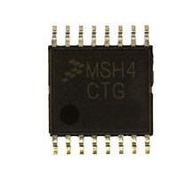
MC9S08SH4CTG Freescale, MC9S08SH4CTG Datasheet - Page 264

MC9S08SH4CTG
Manufacturer Part Number
MC9S08SH4CTG
Description
Manufacturer
Freescale
Datasheet
1.MC9S08SH4CTG.pdf
(338 pages)
Specifications of MC9S08SH4CTG
Cpu Family
HCS08
Device Core Size
8b
Frequency (max)
40MHz
Interface Type
I2C/SCI/SPI
Total Internal Ram Size
256Byte
# I/os (max)
13
Number Of Timers - General Purpose
1
Operating Supply Voltage (typ)
3.3/5V
Operating Supply Voltage (max)
5.5V
Operating Supply Voltage (min)
2.7V
On-chip Adc
8-chx10-bit
Instruction Set Architecture
CISC
Operating Temp Range
-40C to 85C
Operating Temperature Classification
Industrial
Mounting
Surface Mount
Pin Count
16
Package Type
TSSOP
Program Memory Type
Flash
Program Memory Size
4KB
Lead Free Status / RoHS Status
Compliant
Available stocks
Company
Part Number
Manufacturer
Quantity
Price
Company:
Part Number:
MC9S08SH4CTG
Manufacturer:
FREESCAL
Quantity:
96
Company:
Part Number:
MC9S08SH4CTG
Manufacturer:
Freescale
Quantity:
8 727
- Current page: 264 of 338
- Download datasheet (4Mb)
Chapter 16 Timer/PWM Module (S08TPMV3)
264
TPMxCNTH:TPMxCNTL
TPMxMODH:TPMxMODL = 0x0007
TPMxCnVH:TPMxCnVL = 0x0005
EPWM mode
6. Write to TPMxMODH:L registers in BDM mode
7. Update of EPWM signal when CLKSB:CLKSA = 00
(in TPMv2 and TPMv3)
TPMv2 TPMxCHn
CLKSB:CLKSA BITS
TPMv3 TPMxCHn
ELSnB:ELSnA BITS
RESET (active low)
MSnB:MSnA BITS
— TPMxCnVH:L is changed from a non-zero value to 0x0000 [SE110-TPM case 4]
Registers
In the TPM v3 a write to TPMxSC register in BDM mode clears the write coherency mechanism
of TPMxMODH:L registers. Instead, in the TPM v2 this coherency mechanism is not cleared when
there is a write to TPMxSC register.
In the TPM v3 if CLKSB:CLKSA = 00, then the EPWM signal in the channel output is not update
(it is frozen while CLKSB:CLKSA = 00). Instead, in the TPM v2 the EPWM signal is updated at
the next rising edge of bus clock after a write to TPMxCnSC register.
The
after the reset (CLKSB:CLKSA = 00) and if there is a write to TPMxCnSC register.
BUS CLOCK
In this case, the TPM v3 waits for the start of a new PWM period to begin using the new duty
cycle setting. Instead, the TPM v2 changes the channel output at the middle of the current
PWM period (when the count reaches 0x0000).
In this case, the TPM v3 finishes the current PWM period using the old duty cycle setting.
Instead, the TPM v2 finishes the current PWM period using the new duty cycle setting.
Figure 0-1
Figure 0-1. Generation of high-true EPWM signal by TPM v2 and v3 after the reset
CHnF BIT
(TPMxMODH:TPMxMODL))
and
Figure 0-2
00
00
MC9S08SH8 MCU Series Data Sheet, Rev. 3
show when the EPWM signals generated by TPM v2 and TPM v3
00
0
(Section 16.3.3, “TPM Counter Modulo
10
10
1 2 3 4 5 6 7
Freescale Semiconductor
01
0 1
2
...
Related parts for MC9S08SH4CTG
Image
Part Number
Description
Manufacturer
Datasheet
Request
R

Part Number:
Description:
TOWER ELEVATOR BOARDS HARDWARE
Manufacturer:
Freescale Semiconductor
Datasheet:

Part Number:
Description:
TOWER SERIAL I/O HARDWARE
Manufacturer:
Freescale Semiconductor
Datasheet:

Part Number:
Description:
LCD MODULE FOR TWR SYSTEM
Manufacturer:
Freescale Semiconductor
Datasheet:

Part Number:
Description:
DAUGHTER LCD WVGA I.MX51
Manufacturer:
Freescale Semiconductor
Datasheet:

Part Number:
Description:
TOWER SYSTEM BOARD MPC5125
Manufacturer:
Freescale Semiconductor
Datasheet:

Part Number:
Description:
KIT EVALUATION I.MX51
Manufacturer:
Freescale Semiconductor
Datasheet:

Part Number:
Description:
KIT DEVELOPMENT WINCE IMX25
Manufacturer:
Freescale Semiconductor
Datasheet:

Part Number:
Description:
TOWER SYSTEM KIT MPC5125
Manufacturer:
Freescale Semiconductor
Datasheet:

Part Number:
Description:
TOWER SYSTEM BOARD K40X256
Manufacturer:
Freescale Semiconductor
Datasheet:

Part Number:
Description:
TOWER SYSTEM KIT K40X256
Manufacturer:
Freescale Semiconductor
Datasheet:

Part Number:
Description:
Microcontrollers (MCU) MX28 PLATFORM DEV KIT
Manufacturer:
Freescale Semiconductor
Datasheet:

Part Number:
Description:
MCU, MPU & DSP Development Tools IAR KickStart Kit for Kinetis K60
Manufacturer:
Freescale Semiconductor
Datasheet:

Part Number:
Description:
24BIT HDMI MX535/08
Manufacturer:
Freescale Semiconductor
Datasheet:
Part Number:
Description:
Manufacturer:
Freescale Semiconductor, Inc
Datasheet:
Part Number:
Description:
Manufacturer:
Freescale Semiconductor, Inc
Datasheet:


