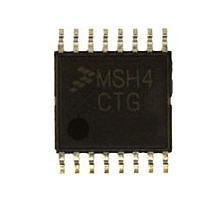
MC9S08SH4CTG Freescale, MC9S08SH4CTG Datasheet - Page 29

MC9S08SH4CTG
Manufacturer Part Number
MC9S08SH4CTG
Description
Manufacturer
Freescale
Datasheet
1.MC9S08SH4CTG.pdf
(338 pages)
Specifications of MC9S08SH4CTG
Cpu Family
HCS08
Device Core Size
8b
Frequency (max)
40MHz
Interface Type
I2C/SCI/SPI
Total Internal Ram Size
256Byte
# I/os (max)
13
Number Of Timers - General Purpose
1
Operating Supply Voltage (typ)
3.3/5V
Operating Supply Voltage (max)
5.5V
Operating Supply Voltage (min)
2.7V
On-chip Adc
8-chx10-bit
Instruction Set Architecture
CISC
Operating Temp Range
-40C to 85C
Operating Temperature Classification
Industrial
Mounting
Surface Mount
Pin Count
16
Package Type
TSSOP
Program Memory Type
Flash
Program Memory Size
4KB
Lead Free Status / RoHS Status
Compliant
Available stocks
Company
Part Number
Manufacturer
Quantity
Price
Company:
Part Number:
MC9S08SH4CTG
Manufacturer:
FREESCAL
Quantity:
96
Company:
Part Number:
MC9S08SH4CTG
Manufacturer:
Freescale
Quantity:
8 727
- Current page: 29 of 338
- Download datasheet (4Mb)
Freescale Semiconductor
1
2
3
4
5
24-pin 20-pin 16-pin
IIC pins can be repositioned using IICPS in SOPT2, default reset locations are on PTA2 and PTA3.
TPM1CHx pins can be repositioned using TPM1PS in SOPT2, default reset locations are on PTA0 and PTB5.
This port pin is part of the ganged output feature. When pin is enabled for ganged output, it will have priority over
all digital modules. The output data, drive strength and slew-rate control of this port pin will follow the configuration
for the PTC0 pin, even in 16-pin packages where PTC0 doesn’t bond out. Ganged output not available in 8-pin
packages.
If ACMP and ADC are both enabled, both will have access to the pin.
Pin is open-drain when configured as output driving high. Pin does not contain a clamp diode to V
not be driven above V
internal gates connected to this pin are pulled to V
10
11
12
13
14
15
16
17
18
19
20
21
22
23
24
1
2
3
4
5
6
7
8
9
Pin Number
10
11
12
13
14
15
16
17
18
19
20
—
—
—
—
3
4
5
6
7
8
9
1
2
—
—
—
—
—
10
11
12
13
14
15
16
—
—
—
3
4
5
6
7
8
9
1
2
DD
. The voltage measured on the internally pulled up RESET will not be pulled to V
Table 2-1. Pin Availability by Package Pin-Count
8-pin
—
—
—
—
—
—
—
—
—
—
—
—
—
—
—
—
3
4
5
6
7
8
1
2
MC9S08SH8 MCU Series Data Sheet, Rev. 3
PTB7
PTB6
PTB5
PTB4
PTC3
PTC2
PTC1
PTC0
PTB3
PTB2
PTB1
PTB0
PTA3
PTA2
PTA1
PTA0
PTA5
PTA4
Port Pin
5
Lowest
SCL
SDA
TPM1CH1
TPM2CH1
PIB3
PIB2
PIB1
PIB0
PIA3
PIA2
PIA1
PIA0
IRQ
ACMPO
DD
Alt 1
1
1
.
2
EXTAL
XTAL
SS
MISO
TPM1CH1
TPM1CH0
MOSI
SPSCK
TxD
RxD
SCL
SDA
TPM2CH0
TPM1CH0
TCLK
Alt 2
1
1
Priority
2
2
2
PTC0
PTC0
PTC0
PTC0
PTC0
PTC0
PTC0
PTC0
Alt 3
3
3
3
3
3
3
3
3
Chapter 2 Pins and Connections
ADP11
ADP10
ADP9
ADP8
ADP7
ADP6
ADP5
ADP4
ADP3
ADP2
ADP1
ADP0
BKGD
Alt 4
Highest
4
4
DD
and should
V
V
ACMP–
ACMP+
MS
DD
SS
RESET
DD
Alt5
. The
4
4
29
Related parts for MC9S08SH4CTG
Image
Part Number
Description
Manufacturer
Datasheet
Request
R

Part Number:
Description:
TOWER ELEVATOR BOARDS HARDWARE
Manufacturer:
Freescale Semiconductor
Datasheet:

Part Number:
Description:
TOWER SERIAL I/O HARDWARE
Manufacturer:
Freescale Semiconductor
Datasheet:

Part Number:
Description:
LCD MODULE FOR TWR SYSTEM
Manufacturer:
Freescale Semiconductor
Datasheet:

Part Number:
Description:
DAUGHTER LCD WVGA I.MX51
Manufacturer:
Freescale Semiconductor
Datasheet:

Part Number:
Description:
TOWER SYSTEM BOARD MPC5125
Manufacturer:
Freescale Semiconductor
Datasheet:

Part Number:
Description:
KIT EVALUATION I.MX51
Manufacturer:
Freescale Semiconductor
Datasheet:

Part Number:
Description:
KIT DEVELOPMENT WINCE IMX25
Manufacturer:
Freescale Semiconductor
Datasheet:

Part Number:
Description:
TOWER SYSTEM KIT MPC5125
Manufacturer:
Freescale Semiconductor
Datasheet:

Part Number:
Description:
TOWER SYSTEM BOARD K40X256
Manufacturer:
Freescale Semiconductor
Datasheet:

Part Number:
Description:
TOWER SYSTEM KIT K40X256
Manufacturer:
Freescale Semiconductor
Datasheet:

Part Number:
Description:
Microcontrollers (MCU) MX28 PLATFORM DEV KIT
Manufacturer:
Freescale Semiconductor
Datasheet:

Part Number:
Description:
MCU, MPU & DSP Development Tools IAR KickStart Kit for Kinetis K60
Manufacturer:
Freescale Semiconductor
Datasheet:

Part Number:
Description:
24BIT HDMI MX535/08
Manufacturer:
Freescale Semiconductor
Datasheet:
Part Number:
Description:
Manufacturer:
Freescale Semiconductor, Inc
Datasheet:
Part Number:
Description:
Manufacturer:
Freescale Semiconductor, Inc
Datasheet:


