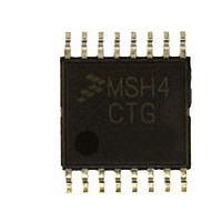
MC9S08SH4CTG Freescale, MC9S08SH4CTG Datasheet - Page 73

MC9S08SH4CTG
Manufacturer Part Number
MC9S08SH4CTG
Description
Manufacturer
Freescale
Datasheet
1.MC9S08SH4CTG.pdf
(338 pages)
Specifications of MC9S08SH4CTG
Cpu Family
HCS08
Device Core Size
8b
Frequency (max)
40MHz
Interface Type
I2C/SCI/SPI
Total Internal Ram Size
256Byte
# I/os (max)
13
Number Of Timers - General Purpose
1
Operating Supply Voltage (typ)
3.3/5V
Operating Supply Voltage (max)
5.5V
Operating Supply Voltage (min)
2.7V
On-chip Adc
8-chx10-bit
Instruction Set Architecture
CISC
Operating Temp Range
-40C to 85C
Operating Temperature Classification
Industrial
Mounting
Surface Mount
Pin Count
16
Package Type
TSSOP
Program Memory Type
Flash
Program Memory Size
4KB
Lead Free Status / RoHS Status
Compliant
Available stocks
Company
Part Number
Manufacturer
Quantity
Price
Company:
Part Number:
MC9S08SH4CTG
Manufacturer:
FREESCAL
Quantity:
96
Company:
Part Number:
MC9S08SH4CTG
Manufacturer:
Freescale
Quantity:
8 727
- Current page: 73 of 338
- Download datasheet (4Mb)
5.7.8
This register is used to report the status of the low voltage warning function, and to configure the stop mode
behavior of the MCU.
Freescale Semiconductor
1
2
Any other Reset:
Power-on Reset:
PPDACK
This bit can be written only one time after power-on reset. Additional writes are ignored.
This bit can be written only one time after reset. Additional writes are ignored.
PPDC
LVWV
PPDF
Field
LVDV
LVD Reset:
5
4
3
2
0
System Power Management Status and Control 2 Register
(SPMSC2)
Figure 5-10. System Power Management Status and Control 2 Register (SPMSC2)
Low-Voltage Detect Voltage Select — This write-once bit selects the low voltage detect (LVD) trip point setting.
It also selects the warning voltage range. See
Low-Voltage Warning Voltage Select — This bit selects the low voltage warning (LVW) trip point voltage. See
Table
Partial Power Down Flag — This read-only status bit indicates that the MCU has recovered from stop2 mode.
0 MCU has not recovered from stop2 mode.
1 MCU recovered from stop2 mode.
Partial Power Down Acknowledge — Writing a 1 to PPDACK clears the PPDF bit
Partial Power Down Control — This write-once bit controls whether stop2 or stop3 mode is selected.
0 Stop3 mode enabled.
1 Stop2, partial power down, mode enabled.
W
R
1
5-12.
See Electrical Characteristics appendix for minimum and maximum values.
0
7
0
0
0
LVDV:LVWV
0:0
0:1
1:0
1:1
= Unimplemented or Reserved
Table 5-12. LVD and LVW trip point typical values
Table 5-11. SPMSC2 Register Field Descriptions
0
0
0
0
6
MC9S08SH8 MCU Series Data Sheet, Rev. 3
LVDV
0
u
u
5
LVW Trip Point
V
V
V
V
LVW0
LVW1
1
LVW2
LVW3
= 2.74 V
= 2.92 V
= 4.3 V
= 4.6 V
LVWV
Table
u
4
0
u
Description
5-12.
Chapter 5 Resets, Interrupts, and General System Control
PPDF
0
0
0
3
LVD Trip Point
V
V
LVD0
LVD1
PPDACK
u = Unaffected by reset
= 2.56 V
= 4.0 V
0
0
0
0
2
1
0
0
0
0
1
PPDC
0
0
0
0
2
73
Related parts for MC9S08SH4CTG
Image
Part Number
Description
Manufacturer
Datasheet
Request
R

Part Number:
Description:
TOWER ELEVATOR BOARDS HARDWARE
Manufacturer:
Freescale Semiconductor
Datasheet:

Part Number:
Description:
TOWER SERIAL I/O HARDWARE
Manufacturer:
Freescale Semiconductor
Datasheet:

Part Number:
Description:
LCD MODULE FOR TWR SYSTEM
Manufacturer:
Freescale Semiconductor
Datasheet:

Part Number:
Description:
DAUGHTER LCD WVGA I.MX51
Manufacturer:
Freescale Semiconductor
Datasheet:

Part Number:
Description:
TOWER SYSTEM BOARD MPC5125
Manufacturer:
Freescale Semiconductor
Datasheet:

Part Number:
Description:
KIT EVALUATION I.MX51
Manufacturer:
Freescale Semiconductor
Datasheet:

Part Number:
Description:
KIT DEVELOPMENT WINCE IMX25
Manufacturer:
Freescale Semiconductor
Datasheet:

Part Number:
Description:
TOWER SYSTEM KIT MPC5125
Manufacturer:
Freescale Semiconductor
Datasheet:

Part Number:
Description:
TOWER SYSTEM BOARD K40X256
Manufacturer:
Freescale Semiconductor
Datasheet:

Part Number:
Description:
TOWER SYSTEM KIT K40X256
Manufacturer:
Freescale Semiconductor
Datasheet:

Part Number:
Description:
Microcontrollers (MCU) MX28 PLATFORM DEV KIT
Manufacturer:
Freescale Semiconductor
Datasheet:

Part Number:
Description:
MCU, MPU & DSP Development Tools IAR KickStart Kit for Kinetis K60
Manufacturer:
Freescale Semiconductor
Datasheet:

Part Number:
Description:
24BIT HDMI MX535/08
Manufacturer:
Freescale Semiconductor
Datasheet:
Part Number:
Description:
Manufacturer:
Freescale Semiconductor, Inc
Datasheet:
Part Number:
Description:
Manufacturer:
Freescale Semiconductor, Inc
Datasheet:


