HW-V5-ML550-UNI-G Xilinx Inc, HW-V5-ML550-UNI-G Datasheet - Page 83
HW-V5-ML550-UNI-G
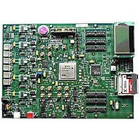
Manufacturer Part Number
HW-V5-ML550-UNI-G
Description
EVALUATION PLATFORM VIRTEX-5
Manufacturer
Xilinx Inc
Series
Virtex™-5 LXTr
Type
FPGAr
Datasheet
1.HW-V5-ML550-UNI-G.pdf
(88 pages)
Specifications of HW-V5-ML550-UNI-G
Contents
Development Platform, Power Supply, Loopback Board, CompactFlash Card, software and documentation
Silicon Manufacturer
Xilinx
Features
64M X 8 DDR SDRAM Memory, Six Samtec LVDS Connectors
Kit Contents
Board, Cable, PSU, CD, Docs
Silicon Family Name
Virtex-5
Silicon Core Number
XC5VLX50T-FFG1136
Rohs Compliant
Yes
Lead Free Status / RoHS Status
Lead free / RoHS Compliant
For Use With/related Products
Virtex™-5 LXT
Lead Free Status / RoHS Status
Lead free / RoHS Compliant, Lead free / RoHS Compliant
Available stocks
Company
Part Number
Manufacturer
Quantity
Price


ML550 Networking Interfaces Platform
UG202 (v1.4) April 18, 2008
R
When presenting byte value 30 hex, character 0 must be displayed. Shifting the value
00110000b (30h) up three positions gives the value 180h or 348d.
Because each character uses eight byte locations, character 0 in the character set starts from
memory location 348 decimal.
For example, character X has byte value 58h or 01011000b. Shifting this value three
positions gives the value 2C0h or 704d.
Figure C-11
data is latched and then shifted left three positions. This shifted value is the start byte for a
counter that outputs an address to the block RAM. The result is a stream of bytes
representing a character for the display.
A small second counter determines when a new character is loaded into the block RAM
address counter.
RAMB16_S9
Addr[10:0]
shows a block diagram of the LCD character generator controller. Character
2047
1280
1279
1024
1023
256
255
0
Figure C-10: Block RAM Organization
www.xilinx.com
Not Used
Not Used
Not Used
D0 - DF
C0 - CF
F0 - FF
E0 - EF
B0 - BF
A0 - AF
70 - 7F
60 - 6F
50 - 5F
40 - 4F
30 - 3F
20 - 2F
10 - 1F
Data[7:0]
Addr
The RAM array is divided in
pages of eight bytes by 16,
forming an array of 128 bytes.
This array represents one
column of standard ASCII table.
A character is stored as:
N-x
N-1
N
0
Hardware Schematic Diagram
0 1 2 3 4 5 6 7 Data
UG202_C_10_050906
Shift
Direction
83
Related parts for HW-V5-ML550-UNI-G
Image
Part Number
Description
Manufacturer
Datasheet
Request
R

Part Number:
Description:
IC CPLD .8K 36MCELL 44-VQFP
Manufacturer:
Xilinx Inc
Datasheet:

Part Number:
Description:
IC CPLD 72MCRCELL 10NS 44VQFP
Manufacturer:
Xilinx Inc
Datasheet:

Part Number:
Description:
IC CPLD 1.6K 72MCELL 64-VQFP
Manufacturer:
Xilinx Inc
Datasheet:

Part Number:
Description:
IC CR-II CPLD 64MCELL 44-VQFP
Manufacturer:
Xilinx Inc
Datasheet:

Part Number:
Description:
IC CPLD 1.6K 72MCELL 100-TQFP
Manufacturer:
Xilinx Inc
Datasheet:

Part Number:
Description:
IC CR-II CPLD 64MCELL 56-BGA
Manufacturer:
Xilinx Inc
Datasheet:

Part Number:
Description:
IC CPLD 72MCRCELL 7.5NS 44VQFP
Manufacturer:
Xilinx Inc
Datasheet:
Part Number:
Description:
IC CR-II CPLD 64MCELL 100-VQFP
Manufacturer:
Xilinx Inc
Datasheet:
Part Number:
Description:
IC CPLD 1.6K 72MCELL 100-TQFP
Manufacturer:
Xilinx Inc
Datasheet:

Part Number:
Description:
IC CPLD 72MCRCELL 7.5NS 64VQFP
Manufacturer:
Xilinx Inc
Datasheet:
Part Number:
Description:
IC CPLD 1.6K 72MCELL 100-TQFP
Manufacturer:
Xilinx Inc
Datasheet:

Part Number:
Description:
IC CPLD 1.5K 64MCELL HP 44-VQFP
Manufacturer:
Xilinx Inc

Part Number:
Description:
IC CPLD 36MCRCELL 15NS 44PLCC
Manufacturer:
Xilinx Inc
Datasheet:

Part Number:
Description:
IC CPLD 36MCRCELL 10NS 44PLCC
Manufacturer:
Xilinx Inc
Datasheet:

Part Number:
Description:
IC CPLD 1.5K 64MCELL HP 44-VQFP
Manufacturer:
Xilinx Inc