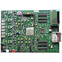
HW-V5-ML550-UNI-G Xilinx Inc, HW-V5-ML550-UNI-G Datasheet - Page 22
HW-V5-ML550-UNI-G
Manufacturer Part Number
HW-V5-ML550-UNI-G
Description
EVALUATION PLATFORM VIRTEX-5
Manufacturer
Xilinx Inc
Series
Virtex™-5 LXTr
Type
FPGAr
Datasheet
1.HW-V5-ML550-UNI-G.pdf
(88 pages)
Specifications of HW-V5-ML550-UNI-G
Contents
Development Platform, Power Supply, Loopback Board, CompactFlash Card, software and documentation
Silicon Manufacturer
Xilinx
Features
64M X 8 DDR SDRAM Memory, Six Samtec LVDS Connectors
Kit Contents
Board, Cable, PSU, CD, Docs
Silicon Family Name
Virtex-5
Silicon Core Number
XC5VLX50T-FFG1136
Rohs Compliant
Yes
Lead Free Status / RoHS Status
Lead free / RoHS Compliant
For Use With/related Products
Virtex™-5 LXT
Lead Free Status / RoHS Status
Lead free / RoHS Compliant, Lead free / RoHS Compliant
Available stocks
Company
Part Number
Manufacturer
Quantity
Price


Chapter 3: Hardware Description
Liquid Crystal Display
22
Table 3-2: SDRAM Memory Interface Signal Descriptions (Continued)
The ML550 Development Board provides an 8-bit interface to a 64 x 128 LCD panel
(DisplayTechQ 64128E-FC-BC-3LP, 64 x 128). This display was chosen because of its
possible use in embedded systems.
operation in detail.
Table 3-3
the ML550 Development Board.
Table 3-3: LCD Interface Signal Descriptions
Notes:
1. Because DQS0 is not located on a clock capable I/O pin, the Xilinx MIG tool cannot be used to
Signal Name
DQ2
DQ3
DQ4
DQ5
DQ6
DQ7
DQS0
BA0
BA1
DM0
CSn
RASn
CASn
WEn
CLK_P
CLK_N
CKE
V
V
MI
DB7
Signal Name
SS
DD
generate a SDRAM memory controller for the 64M x 8 SDRAM on the ML550 board.
(1)
describes the LCD interface signal descriptions for the FFG1136 package used on
Data 2
Data 3
Data 4
Data 5
Data 6
Data 7
DQ Strobe
Bank Select 0
Bank Select 1
Write Mask
Chip Select
Row Address Strobe
Column Address Strobe
Write Enable
Positive Clock
Negative Clock
Clock Enable
LCD Pin
1
2
3
4
Number
www.xilinx.com
Description
GND
3.3V DC
H = 6800 CPU, L = 8080 CPU
LCD Data Bit 7
Appendix C, “LCD Interface,”
Description
ML550 Networking Interfaces Platform
(FFG1136 Package, Bank 12)
F5
R11
N7
N8
M5
M6
T9
G6
T11
G7
E7
U7
T8
E6
H7
J7
U10
(FFG1136 Package, Bank 13)
Ground
Logic Supply
Pull-up R14 to 3.3V
AK33
FPGA Pin Number
UG202 (v1.4) April 18, 2008
FPGA Pin Number
describes the LCD
R
Related parts for HW-V5-ML550-UNI-G
Image
Part Number
Description
Manufacturer
Datasheet
Request
R

Part Number:
Description:
IC CPLD .8K 36MCELL 44-VQFP
Manufacturer:
Xilinx Inc
Datasheet:

Part Number:
Description:
IC CPLD 72MCRCELL 10NS 44VQFP
Manufacturer:
Xilinx Inc
Datasheet:

Part Number:
Description:
IC CPLD 1.6K 72MCELL 64-VQFP
Manufacturer:
Xilinx Inc
Datasheet:

Part Number:
Description:
IC CR-II CPLD 64MCELL 44-VQFP
Manufacturer:
Xilinx Inc
Datasheet:

Part Number:
Description:
IC CPLD 1.6K 72MCELL 100-TQFP
Manufacturer:
Xilinx Inc
Datasheet:

Part Number:
Description:
IC CR-II CPLD 64MCELL 56-BGA
Manufacturer:
Xilinx Inc
Datasheet:

Part Number:
Description:
IC CPLD 72MCRCELL 7.5NS 44VQFP
Manufacturer:
Xilinx Inc
Datasheet:
Part Number:
Description:
IC CR-II CPLD 64MCELL 100-VQFP
Manufacturer:
Xilinx Inc
Datasheet:
Part Number:
Description:
IC CPLD 1.6K 72MCELL 100-TQFP
Manufacturer:
Xilinx Inc
Datasheet:

Part Number:
Description:
IC CPLD 72MCRCELL 7.5NS 64VQFP
Manufacturer:
Xilinx Inc
Datasheet:
Part Number:
Description:
IC CPLD 1.6K 72MCELL 100-TQFP
Manufacturer:
Xilinx Inc
Datasheet:

Part Number:
Description:
IC CPLD 1.5K 64MCELL HP 44-VQFP
Manufacturer:
Xilinx Inc

Part Number:
Description:
IC CPLD 36MCRCELL 15NS 44PLCC
Manufacturer:
Xilinx Inc
Datasheet:

Part Number:
Description:
IC CPLD 36MCRCELL 10NS 44PLCC
Manufacturer:
Xilinx Inc
Datasheet:

Part Number:
Description:
IC CPLD 1.5K 64MCELL HP 44-VQFP
Manufacturer:
Xilinx Inc