HW-V5-ML550-UNI-G Xilinx Inc, HW-V5-ML550-UNI-G Datasheet - Page 30
HW-V5-ML550-UNI-G
Manufacturer Part Number
HW-V5-ML550-UNI-G
Description
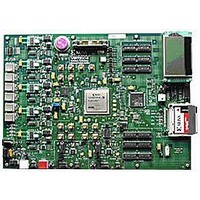
EVALUATION PLATFORM VIRTEX-5
Manufacturer
Xilinx Inc
Series
Virtex™-5 LXTr
Type
FPGAr
Datasheet
1.HW-V5-ML550-UNI-G.pdf
(88 pages)
Specifications of HW-V5-ML550-UNI-G
Contents
Development Platform, Power Supply, Loopback Board, CompactFlash Card, software and documentation
Silicon Manufacturer
Xilinx
Features
64M X 8 DDR SDRAM Memory, Six Samtec LVDS Connectors
Kit Contents
Board, Cable, PSU, CD, Docs
Silicon Family Name
Virtex-5
Silicon Core Number
XC5VLX50T-FFG1136
Rohs Compliant
Yes
Lead Free Status / RoHS Status
Lead free / RoHS Compliant
For Use With/related Products
Virtex™-5 LXT
Lead Free Status / RoHS Status
Lead free / RoHS Compliant, Lead free / RoHS Compliant
Available stocks
Company
Part Number
Manufacturer
Quantity
Price


Chapter 3: Hardware Description
Table 3-9: Voltage Regulators VR1 through VR5
30
Notes:
1. ±5% margin limit.
V
V
System 3.3V
System 2.5V
V
Regulator
CCAUX
CCINT
CCO
VR1
VR2
VR3
VR4
VR5
2.5V
1.0V
2.5V
Jumper
Inhibit
P14
P21
P30
P38
P4
Connector
Test Point
The TI PTH05000 regulator module requires a fixed 5V input. The output is adjustable over
a range of 0.9V to 3.6V by changing the resistor tied between pin 4 and GND.
Table 3-10
Table 3-11
Table 3-10: Voltage Regulator Output Select VR_SEL
Notes:
1. ±5% margin limit.
2. At power-on, FPGA_RESETB (FPGA U9.W34) is not driven and is pulled down by a 4.7 K resistor.
3. At power-on, V
4. To enable margin control, the U9.W34 FPGA_RESETB pin must be driven High.
5. To select other than the nominal output, set up the margin % on VR_SEL[3:0], then strobe the
P13
P16
P22
P33
appropriate STB_* from Low to High to Low to clock the value into the latch.
P1
Jumper OFF = Enabled
Jumper ON = Inhibited
3
0
0
0
0
1
1
1
1
-
lists the pin locations for VR_SEL[3:0].
STB_VCCAUX2V5
shows the VR_SEL[3:0] settings used to control the voltage regulator outputs.
STB_VCCINT1V0
(FPGA U9:AD4)
(FPGA U9:AA6)
(FPGA U9:AD6)
(FPGA U9:AD5)
Margin Control
STB_VCCO2V5
(FPGA U9:Y7)
STB_SYS3V3
STB_SYS2V5
Strobes
REG
defaults to the nominal output.
www.xilinx.com
2
0
0
1
1
0
0
1
1
-
VR_SEL[3:0]
–10% –7.5% –5% –2.5% Nom +2.5% +5% +7.5% +10%
2.97
0.90
2.25
2.25
2.25
3.05
0.93
2.31
2.31
2.31
3.14
0.95
2.38
2.38
2.38
1
0
1
0
1
0
1
0
1
-
V
OUT
3.22
0.98
2.44
2.44
2.44
Target Voltage (V)
ML550 Networking Interfaces Platform
3.30 3.383 3.465
1.00 1.025
2.50 2.563 2.625
2.50 2.563 2.625
2.50 2.563 2.625
0
1
1
1
1
0
1
1
1
1
UG202 (v1.4) April 18, 2008
(1)
1.05
Selected
Nominal
3.548
1.075
2.688
2.688
2.688
+2.5%
+7.5%
–7.5%
–2.5%
+10%
–10%
V
–5%
+5%
OUT
3.63
2.75
2.75
2.75
(1)
1.1
R
Related parts for HW-V5-ML550-UNI-G
Image
Part Number
Description
Manufacturer
Datasheet
Request
R

Part Number:
Description:
IC CPLD .8K 36MCELL 44-VQFP
Manufacturer:
Xilinx Inc
Datasheet:

Part Number:
Description:
IC CPLD 72MCRCELL 10NS 44VQFP
Manufacturer:
Xilinx Inc
Datasheet:

Part Number:
Description:
IC CPLD 1.6K 72MCELL 64-VQFP
Manufacturer:
Xilinx Inc
Datasheet:

Part Number:
Description:
IC CR-II CPLD 64MCELL 44-VQFP
Manufacturer:
Xilinx Inc
Datasheet:

Part Number:
Description:
IC CPLD 1.6K 72MCELL 100-TQFP
Manufacturer:
Xilinx Inc
Datasheet:

Part Number:
Description:
IC CR-II CPLD 64MCELL 56-BGA
Manufacturer:
Xilinx Inc
Datasheet:

Part Number:
Description:
IC CPLD 72MCRCELL 7.5NS 44VQFP
Manufacturer:
Xilinx Inc
Datasheet:
Part Number:
Description:
IC CR-II CPLD 64MCELL 100-VQFP
Manufacturer:
Xilinx Inc
Datasheet:
Part Number:
Description:
IC CPLD 1.6K 72MCELL 100-TQFP
Manufacturer:
Xilinx Inc
Datasheet:

Part Number:
Description:
IC CPLD 72MCRCELL 7.5NS 64VQFP
Manufacturer:
Xilinx Inc
Datasheet:
Part Number:
Description:
IC CPLD 1.6K 72MCELL 100-TQFP
Manufacturer:
Xilinx Inc
Datasheet:

Part Number:
Description:
IC CPLD 1.5K 64MCELL HP 44-VQFP
Manufacturer:
Xilinx Inc

Part Number:
Description:
IC CPLD 36MCRCELL 15NS 44PLCC
Manufacturer:
Xilinx Inc
Datasheet:

Part Number:
Description:
IC CPLD 36MCRCELL 10NS 44PLCC
Manufacturer:
Xilinx Inc
Datasheet:

Part Number:
Description:
IC CPLD 1.5K 64MCELL HP 44-VQFP
Manufacturer:
Xilinx Inc