HW-V5-ML550-UNI-G Xilinx Inc, HW-V5-ML550-UNI-G Datasheet - Page 80
HW-V5-ML550-UNI-G
Manufacturer Part Number
HW-V5-ML550-UNI-G
Description
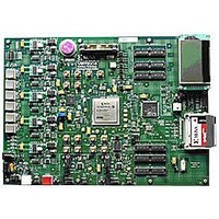
EVALUATION PLATFORM VIRTEX-5
Manufacturer
Xilinx Inc
Series
Virtex™-5 LXTr
Type
FPGAr
Datasheet
1.HW-V5-ML550-UNI-G.pdf
(88 pages)
Specifications of HW-V5-ML550-UNI-G
Contents
Development Platform, Power Supply, Loopback Board, CompactFlash Card, software and documentation
Silicon Manufacturer
Xilinx
Features
64M X 8 DDR SDRAM Memory, Six Samtec LVDS Connectors
Kit Contents
Board, Cable, PSU, CD, Docs
Silicon Family Name
Virtex-5
Silicon Core Number
XC5VLX50T-FFG1136
Rohs Compliant
Yes
Lead Free Status / RoHS Status
Lead free / RoHS Compliant
For Use With/related Products
Virtex™-5 LXT
Lead Free Status / RoHS Status
Lead free / RoHS Compliant, Lead free / RoHS Compliant
Available stocks
Company
Part Number
Manufacturer
Quantity
Price


Appendix C: LCD Interface
80
Design Examples
LCD Panel Used in Full Graphics Mode
The LCD controller RAM has eight 132-byte pages (in fact, there are nine pages; page 9 is
special). Each page is one-byte wide. If all the pages are put in one memory block, then the
needed space is 8 pages x 8 bits x 132 pixels or 8448 bits (1056 bytes).
One Virtex-4 block RAM can be configured as 8+1 by 2048.
One block RAM can be used to store one complete pixel view of the LCD panel. There is
enough space left for commands.
The ninth bit in the block RAM memory indicates whether the data in the block RAM is
real data to be displayed or is a command for the controller.
The interface to the LCD panel is slow. The E signal can be used as the controller clock
signal. This signal has a minimum cycle time of 400 ns for displaying 8 bits (equal to 8 dots)
on the LCD. One full page of the display takes up to 132 x 400 ns = 52.8 s. Updating the
full display takes 52.8 s x 8 = 423 s.
If using the dual port and data width capabilities of the block RAM, writes to the block
RAM can be 32 bits (+4 control bits), and reads from the block RAM on the LCD side can be
8 bits (1 control bit). An entire LCD page is updated in 33 write operations.
The interface on the LCD panel side sequentially reads the block RAM and thus updates
the screen contiguously (like a television screen). The controller (microcontroller or other)
side of the block RAM can be written at any time.
The write operation happens on the rising edge of the clock, and the read (LCD update)
happens on the falling edge of the clock. Normally, write and read operations at the same
address give corrupt read data when the read and write clock edges do not respect the
clock-to-clock setup timing. This problem is solved by using both edges of the clock.
A state machine is used to provide correct timing of the signals on the LCD panel side. The
panel can be used in write-only mode or in read/write mode. Most of the time LCD panels
operate in write-only mode.
At first the block RAM must be initialized with some data (instructions to the LCD) to
make the LCD operate correctly.
www.xilinx.com
ML550 Networking Interfaces Platform
UG202 (v1.4) April 18, 2008
R
Related parts for HW-V5-ML550-UNI-G
Image
Part Number
Description
Manufacturer
Datasheet
Request
R

Part Number:
Description:
IC CPLD .8K 36MCELL 44-VQFP
Manufacturer:
Xilinx Inc
Datasheet:

Part Number:
Description:
IC CPLD 72MCRCELL 10NS 44VQFP
Manufacturer:
Xilinx Inc
Datasheet:

Part Number:
Description:
IC CPLD 1.6K 72MCELL 64-VQFP
Manufacturer:
Xilinx Inc
Datasheet:

Part Number:
Description:
IC CR-II CPLD 64MCELL 44-VQFP
Manufacturer:
Xilinx Inc
Datasheet:

Part Number:
Description:
IC CPLD 1.6K 72MCELL 100-TQFP
Manufacturer:
Xilinx Inc
Datasheet:

Part Number:
Description:
IC CR-II CPLD 64MCELL 56-BGA
Manufacturer:
Xilinx Inc
Datasheet:

Part Number:
Description:
IC CPLD 72MCRCELL 7.5NS 44VQFP
Manufacturer:
Xilinx Inc
Datasheet:
Part Number:
Description:
IC CR-II CPLD 64MCELL 100-VQFP
Manufacturer:
Xilinx Inc
Datasheet:
Part Number:
Description:
IC CPLD 1.6K 72MCELL 100-TQFP
Manufacturer:
Xilinx Inc
Datasheet:

Part Number:
Description:
IC CPLD 72MCRCELL 7.5NS 64VQFP
Manufacturer:
Xilinx Inc
Datasheet:
Part Number:
Description:
IC CPLD 1.6K 72MCELL 100-TQFP
Manufacturer:
Xilinx Inc
Datasheet:

Part Number:
Description:
IC CPLD 1.5K 64MCELL HP 44-VQFP
Manufacturer:
Xilinx Inc

Part Number:
Description:
IC CPLD 36MCRCELL 15NS 44PLCC
Manufacturer:
Xilinx Inc
Datasheet:

Part Number:
Description:
IC CPLD 36MCRCELL 10NS 44PLCC
Manufacturer:
Xilinx Inc
Datasheet:

Part Number:
Description:
IC CPLD 1.5K 64MCELL HP 44-VQFP
Manufacturer:
Xilinx Inc