HW-V5-ML550-UNI-G Xilinx Inc, HW-V5-ML550-UNI-G Datasheet - Page 41
HW-V5-ML550-UNI-G
Manufacturer Part Number
HW-V5-ML550-UNI-G
Description
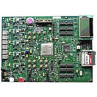
EVALUATION PLATFORM VIRTEX-5
Manufacturer
Xilinx Inc
Series
Virtex™-5 LXTr
Type
FPGAr
Datasheet
1.HW-V5-ML550-UNI-G.pdf
(88 pages)
Specifications of HW-V5-ML550-UNI-G
Contents
Development Platform, Power Supply, Loopback Board, CompactFlash Card, software and documentation
Silicon Manufacturer
Xilinx
Features
64M X 8 DDR SDRAM Memory, Six Samtec LVDS Connectors
Kit Contents
Board, Cable, PSU, CD, Docs
Silicon Family Name
Virtex-5
Silicon Core Number
XC5VLX50T-FFG1136
Rohs Compliant
Yes
Lead Free Status / RoHS Status
Lead free / RoHS Compliant
For Use With/related Products
Virtex™-5 LXT
Lead Free Status / RoHS Status
Lead free / RoHS Compliant, Lead free / RoHS Compliant
Available stocks
Company
Part Number
Manufacturer
Quantity
Price


ML550 Networking Interfaces Platform
UG202 (v1.4) April 18, 2008
30,U9.T18
19,U10.2
19,P39.2
34,U9.P34
34,U9.L33
R
SM_AVDD
REF_2V5_OUT
SM_GPIO2
SM_GPIO4
J19 Mezzanine Board Connector
D_OUT_BUSY_0_AD15
PROGRAM_B_0_M22
VCC2V5
HSWAPEN_0_M23
Bank 0
R_FUSE_0_AC23
RDWR_B_0_N23
J19 is provided to enable users to develop signal conditioning boards and take advantage
of the System Monitor VP/VN input channel on FPGA pins U18/V17. The J19 connections
to the FPGA are shown in
to provide general purpose I/O, as detailed in
pinout details are shown in
U9
VREFN_0_U17
VREFP_0_V18
INIT_B_0_N14
VBATT_0_L23
DONE_0_M15
TDO_0_AD14
TMS_0_AC14
CCLK_0_N15
AVDD_0_T18
TCK_0_AB15
CS_B_0_N22
VFS_0_AB23
AVSS_0_T17
Figure 3-20: J19 Mezzanine Board Connector (Sheet 30)
DXN_0_W17
TDI_0_AC15
D_IN_0_P15
DXP_0_W18
M0_0_AD21
M1_0_AC22
M2_0_AD22
VP_0_U18
VN_0_V17
0.01UF
C79
VP_SM
VN_SM
AC15
AD14
AC14
AB15
AD21
AC22
AD22
AD15
P15
M22
N15
N14
M15
N22
N23
AC23
M23
AB23
L23
W18
W17
V18
U17
U18
V17
T18
T17
R452
100R
DF9_17S_1V
11
13
15
17
1
2
1
3
5
7
9
1
2
J19
1
2
2
4
6
8
10
12
14
16
FPGA_PROGB
CCLK
FPGA_INIT_B
FPGA_DONE
R77
4.7K
1
2
D
R453
100R
M0
M1
M2
DIN
HSWAPEN
VBATT
www.xilinx.com
Figure
Table 3-15, page
1
2
R72
4.7K
3-20. Four FPGA Bank 11 GPIO pins are connected to J19
GNDA
A
ML550 System Monitor and Power Monitor Support
TD_P
TD_N
1
2
VCC5
1
2
SM_GPIO1
SM_GPIO3
R81
DNA
C74
0.01UF
P41.6
VCC2V5
42.
1
2
Figure 3-20
R94
DNA
2
SYSACE_TDO
SYSACE_TDI
FPGA_TMS
FPGA_TCK
P27
34,U9.N34
34,U9.M32
1
2
1
30,D23.3
SM_VREF_P
C76
0.01 F
and
Table 3-13, page
from
System ACE
Controller
19,L1.1
UG202_3_20_041508
VCC2V5
34. J19
2
1
4.7K
R135
41
Related parts for HW-V5-ML550-UNI-G
Image
Part Number
Description
Manufacturer
Datasheet
Request
R

Part Number:
Description:
IC CPLD .8K 36MCELL 44-VQFP
Manufacturer:
Xilinx Inc
Datasheet:

Part Number:
Description:
IC CPLD 72MCRCELL 10NS 44VQFP
Manufacturer:
Xilinx Inc
Datasheet:

Part Number:
Description:
IC CPLD 1.6K 72MCELL 64-VQFP
Manufacturer:
Xilinx Inc
Datasheet:

Part Number:
Description:
IC CR-II CPLD 64MCELL 44-VQFP
Manufacturer:
Xilinx Inc
Datasheet:

Part Number:
Description:
IC CPLD 1.6K 72MCELL 100-TQFP
Manufacturer:
Xilinx Inc
Datasheet:

Part Number:
Description:
IC CR-II CPLD 64MCELL 56-BGA
Manufacturer:
Xilinx Inc
Datasheet:

Part Number:
Description:
IC CPLD 72MCRCELL 7.5NS 44VQFP
Manufacturer:
Xilinx Inc
Datasheet:
Part Number:
Description:
IC CR-II CPLD 64MCELL 100-VQFP
Manufacturer:
Xilinx Inc
Datasheet:
Part Number:
Description:
IC CPLD 1.6K 72MCELL 100-TQFP
Manufacturer:
Xilinx Inc
Datasheet:

Part Number:
Description:
IC CPLD 72MCRCELL 7.5NS 64VQFP
Manufacturer:
Xilinx Inc
Datasheet:
Part Number:
Description:
IC CPLD 1.6K 72MCELL 100-TQFP
Manufacturer:
Xilinx Inc
Datasheet:

Part Number:
Description:
IC CPLD 1.5K 64MCELL HP 44-VQFP
Manufacturer:
Xilinx Inc

Part Number:
Description:
IC CPLD 36MCRCELL 15NS 44PLCC
Manufacturer:
Xilinx Inc
Datasheet:

Part Number:
Description:
IC CPLD 36MCRCELL 10NS 44PLCC
Manufacturer:
Xilinx Inc
Datasheet:

Part Number:
Description:
IC CPLD 1.5K 64MCELL HP 44-VQFP
Manufacturer:
Xilinx Inc