HW-V5-ML550-UNI-G Xilinx Inc, HW-V5-ML550-UNI-G Datasheet - Page 20
HW-V5-ML550-UNI-G
Manufacturer Part Number
HW-V5-ML550-UNI-G
Description
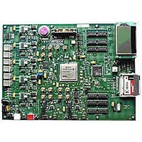
EVALUATION PLATFORM VIRTEX-5
Manufacturer
Xilinx Inc
Series
Virtex™-5 LXTr
Type
FPGAr
Datasheet
1.HW-V5-ML550-UNI-G.pdf
(88 pages)
Specifications of HW-V5-ML550-UNI-G
Contents
Development Platform, Power Supply, Loopback Board, CompactFlash Card, software and documentation
Silicon Manufacturer
Xilinx
Features
64M X 8 DDR SDRAM Memory, Six Samtec LVDS Connectors
Kit Contents
Board, Cable, PSU, CD, Docs
Silicon Family Name
Virtex-5
Silicon Core Number
XC5VLX50T-FFG1136
Rohs Compliant
Yes
Lead Free Status / RoHS Status
Lead free / RoHS Compliant
For Use With/related Products
Virtex™-5 LXT
Lead Free Status / RoHS Status
Lead free / RoHS Compliant, Lead free / RoHS Compliant
Available stocks
Company
Part Number
Manufacturer
Quantity
Price


Chapter 3: Hardware Description
Clock Generation
Table 3-1: Clock Generation – ML550 Rev 01 Board
20
Epson SG8002CA
Epson EG2121CA
Epson EG2121CA
Epson EG2121CA
ICS8442AY
ICS8442AY
SMA Connector
SMA Connector
SMA Connector
SMA Connector
Clock Source
Component
Designator
Reference
U18
U19
Y1
Y2
Y3
Y4
J1
J2
J3
J4
The clock generation section of the ML550 Development Board provides all necessary
clocks for the Virtex-5 FPGA. Eight clock sources are provided:
The differential SMA clock inputs are connected to the global clock inputs of the FPGA. An
onboard 200-MHz oscillator calibrates the I/O delay, and an onboard 250-MHz oscillator is
provided for general use.
The two ICS8442 clock synthesizer devices output differential LVDS clocks in the
31.25 MHz to 700 MHz range.
The on-chip LVDS differential terminator is recommended for use in designs. The clock is
received by an IBUFGDS module, and beneath that module instantiation, the synthesis
attribute DIFF_TERM must be set to TRUE. Refer to the Virtex-5 FPGA User Guide (UG190)
for information and examples using SelectIO primitives for LVDS inputs.
Table 3-1
Epson EG2121CA 2.5V 250-MHz differential LVPECL oscillator (Y4) for general use
Epson EG2121CA 2.5V 200-MHz differential LVPECL oscillator (Y3) for Virtex-5
FPGA ISERDES support
Epson EG2121CA 2.5V 133-MHz differential LVDS oscillator (Y2) for DDR memory
interface
Epson SG8002CA 3.3V 33-MHz LVCMOS single-ended oscillator (Y1) for SystemAce
device (U13)
Two differential SMA clock inputs (CLOCK-1: J3, J1 and CLOCK-2: J4, J2)
Two clock synthesizer ICS8442 devices (U18,U19)
to 700 MHz 3.3V LVDS Differential #2 CLKMOD1_FOUT1_P and N
to 700 MHz 3.3V LVDS Differential #2 LVDSCLKMOD2B_P and N
Frequency
31.25 MHz 3.3V LVDS Differential #1 LVDSCLKMOD1_P and N
31.25 MHz 3.3V LVDS Differential #1 LVDSCLKMOD2A_P and N
133 MHz
200 MHz
250 MHz
Output
33 MHz
shows the clock generation components for the ML550 board.
3.3V LVCMOS
Single-Ended
2.5V LVDS Differential
2.5V LVPECL Differential OSC_200M_P and N
2.5V LVPECL Differential OSC_250M_P and N
Output Type
www.xilinx.com
SYSACE_CLK
OSC_133M_P and N
SMA_CLK1_P
SMA_CLK1_N
SMA_CLK2_P
SMA_CLK2_N
Signal Name
ML550 Networking Interfaces Platform
UG202 (v1.4) April 18, 2008
AH18
AK28
AD10
AB30
AF18
N/A
N/A
H17
V33
FPGA Pin #
L19
J13
R7
P
AG17
AC30
AK27
AD11
AE18
N/A
N/A
N/A
K19
H18
J14
R8
N
Bank
N/A
13
12
17
21
22
22
3
3
4
4
4
R
Related parts for HW-V5-ML550-UNI-G
Image
Part Number
Description
Manufacturer
Datasheet
Request
R

Part Number:
Description:
IC CPLD .8K 36MCELL 44-VQFP
Manufacturer:
Xilinx Inc
Datasheet:

Part Number:
Description:
IC CPLD 72MCRCELL 10NS 44VQFP
Manufacturer:
Xilinx Inc
Datasheet:

Part Number:
Description:
IC CPLD 1.6K 72MCELL 64-VQFP
Manufacturer:
Xilinx Inc
Datasheet:

Part Number:
Description:
IC CR-II CPLD 64MCELL 44-VQFP
Manufacturer:
Xilinx Inc
Datasheet:

Part Number:
Description:
IC CPLD 1.6K 72MCELL 100-TQFP
Manufacturer:
Xilinx Inc
Datasheet:

Part Number:
Description:
IC CR-II CPLD 64MCELL 56-BGA
Manufacturer:
Xilinx Inc
Datasheet:

Part Number:
Description:
IC CPLD 72MCRCELL 7.5NS 44VQFP
Manufacturer:
Xilinx Inc
Datasheet:
Part Number:
Description:
IC CR-II CPLD 64MCELL 100-VQFP
Manufacturer:
Xilinx Inc
Datasheet:
Part Number:
Description:
IC CPLD 1.6K 72MCELL 100-TQFP
Manufacturer:
Xilinx Inc
Datasheet:

Part Number:
Description:
IC CPLD 72MCRCELL 7.5NS 64VQFP
Manufacturer:
Xilinx Inc
Datasheet:
Part Number:
Description:
IC CPLD 1.6K 72MCELL 100-TQFP
Manufacturer:
Xilinx Inc
Datasheet:

Part Number:
Description:
IC CPLD 1.5K 64MCELL HP 44-VQFP
Manufacturer:
Xilinx Inc

Part Number:
Description:
IC CPLD 36MCRCELL 15NS 44PLCC
Manufacturer:
Xilinx Inc
Datasheet:

Part Number:
Description:
IC CPLD 36MCRCELL 10NS 44PLCC
Manufacturer:
Xilinx Inc
Datasheet:

Part Number:
Description:
IC CPLD 1.5K 64MCELL HP 44-VQFP
Manufacturer:
Xilinx Inc