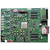
HW-V5-ML550-UNI-G Xilinx Inc, HW-V5-ML550-UNI-G Datasheet - Page 23
HW-V5-ML550-UNI-G
Manufacturer Part Number
HW-V5-ML550-UNI-G
Description
EVALUATION PLATFORM VIRTEX-5
Manufacturer
Xilinx Inc
Series
Virtex™-5 LXTr
Type
FPGAr
Datasheet
1.HW-V5-ML550-UNI-G.pdf
(88 pages)
Specifications of HW-V5-ML550-UNI-G
Contents
Development Platform, Power Supply, Loopback Board, CompactFlash Card, software and documentation
Silicon Manufacturer
Xilinx
Features
64M X 8 DDR SDRAM Memory, Six Samtec LVDS Connectors
Kit Contents
Board, Cable, PSU, CD, Docs
Silicon Family Name
Virtex-5
Silicon Core Number
XC5VLX50T-FFG1136
Rohs Compliant
Yes
Lead Free Status / RoHS Status
Lead free / RoHS Compliant
For Use With/related Products
Virtex™-5 LXT
Lead Free Status / RoHS Status
Lead free / RoHS Compliant, Lead free / RoHS Compliant
Available stocks
Company
Part Number
Manufacturer
Quantity
Price


ML550 Networking Interfaces Platform
UG202 (v1.4) April 18, 2008
Display Hardware Design
R
Table 3-3: LCD Interface Signal Descriptions (Continued)
The LCD can display alphanumeric (ASCII) information; however, a hardware character
generator must be designed in the FPGA fabric in order to display the characters on the
LCD screen. A character-type display (with on-board character generator) can also be
connected because the graphical LCD has the same interface as many character-type LCD
panels.
The I/Os of the FPGA function at 2.5V. The FPGA is connected to the graphic LCD display
through a set of voltage-level converting devices. These switches translate the 2.5V I/O
signals to the 3.3V signals that the LCD display requires.
Control for the LCD panel is based on the KS0713 controller from Samsung. The KS0713 is
a 65-column, 132-segment driver-controller device for graphic dot matrix LCD display
systems. The chip accepts serial or parallel display data. The 8-bit parallel interface is
compatible with most LCD panel manufacturers. The serial connection mode is write only.
Extra features added to the interface in addition to the normal parallel signals are:
The interface also contains the following built-in options for the display and controller:
DB6
DB5
DB4
DB3
DB2
DB1
DB0
E
R/W
RS
RST
CS1B
LED +
LED –
LCD_BL_ON
Signal Name
Intel or Motorola compatible interface
External reset of the chip
External chip select
On-chip oscillator circuitry
On-chip voltage converter (x2, x3, x4, and x5)
LCD Pin
5
6
7
8
9
10
11
12
13
14
15
16
17
18
N/A
Number
www.xilinx.com
LCD Data Bit 6
LCD Data Bit 5
LCD Data Bit 4
LCD Data Bit 3
LCD Data Bit 2
LCD Data Bit 1
LCD Data Bit 0
LCD Enable
LCD Write
LCD Register Select
LCD Reset
LCD Chip Select
LCD Backlight Anode
LCD Backlight Cathode
LCD Backlight Control
Description
(FFG1136 Package, Bank 13)
AG32
AH32
AJ32
AK32
AL34
AL33
AM33
AN33
AN32
AP32
AM32
AN34
Ground
AK34
Ctrl. Transistor Q1
FPGA Pin Number
Liquid Crystal Display
23
Related parts for HW-V5-ML550-UNI-G
Image
Part Number
Description
Manufacturer
Datasheet
Request
R

Part Number:
Description:
IC CPLD .8K 36MCELL 44-VQFP
Manufacturer:
Xilinx Inc
Datasheet:

Part Number:
Description:
IC CPLD 72MCRCELL 10NS 44VQFP
Manufacturer:
Xilinx Inc
Datasheet:

Part Number:
Description:
IC CPLD 1.6K 72MCELL 64-VQFP
Manufacturer:
Xilinx Inc
Datasheet:

Part Number:
Description:
IC CR-II CPLD 64MCELL 44-VQFP
Manufacturer:
Xilinx Inc
Datasheet:

Part Number:
Description:
IC CPLD 1.6K 72MCELL 100-TQFP
Manufacturer:
Xilinx Inc
Datasheet:

Part Number:
Description:
IC CR-II CPLD 64MCELL 56-BGA
Manufacturer:
Xilinx Inc
Datasheet:

Part Number:
Description:
IC CPLD 72MCRCELL 7.5NS 44VQFP
Manufacturer:
Xilinx Inc
Datasheet:
Part Number:
Description:
IC CR-II CPLD 64MCELL 100-VQFP
Manufacturer:
Xilinx Inc
Datasheet:
Part Number:
Description:
IC CPLD 1.6K 72MCELL 100-TQFP
Manufacturer:
Xilinx Inc
Datasheet:

Part Number:
Description:
IC CPLD 72MCRCELL 7.5NS 64VQFP
Manufacturer:
Xilinx Inc
Datasheet:
Part Number:
Description:
IC CPLD 1.6K 72MCELL 100-TQFP
Manufacturer:
Xilinx Inc
Datasheet:

Part Number:
Description:
IC CPLD 1.5K 64MCELL HP 44-VQFP
Manufacturer:
Xilinx Inc

Part Number:
Description:
IC CPLD 36MCRCELL 15NS 44PLCC
Manufacturer:
Xilinx Inc
Datasheet:

Part Number:
Description:
IC CPLD 36MCRCELL 10NS 44PLCC
Manufacturer:
Xilinx Inc
Datasheet:

Part Number:
Description:
IC CPLD 1.5K 64MCELL HP 44-VQFP
Manufacturer:
Xilinx Inc