HW-V5-ML550-UNI-G Xilinx Inc, HW-V5-ML550-UNI-G Datasheet - Page 26
HW-V5-ML550-UNI-G
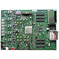
Manufacturer Part Number
HW-V5-ML550-UNI-G
Description
EVALUATION PLATFORM VIRTEX-5
Manufacturer
Xilinx Inc
Series
Virtex™-5 LXTr
Type
FPGAr
Datasheet
1.HW-V5-ML550-UNI-G.pdf
(88 pages)
Specifications of HW-V5-ML550-UNI-G
Contents
Development Platform, Power Supply, Loopback Board, CompactFlash Card, software and documentation
Silicon Manufacturer
Xilinx
Features
64M X 8 DDR SDRAM Memory, Six Samtec LVDS Connectors
Kit Contents
Board, Cable, PSU, CD, Docs
Silicon Family Name
Virtex-5
Silicon Core Number
XC5VLX50T-FFG1136
Rohs Compliant
Yes
Lead Free Status / RoHS Status
Lead free / RoHS Compliant
For Use With/related Products
Virtex™-5 LXT
Lead Free Status / RoHS Status
Lead free / RoHS Compliant, Lead free / RoHS Compliant
Available stocks
Company
Part Number
Manufacturer
Quantity
Price


Chapter 3: Hardware Description
Configuration INIT and DONE LEDs
User Push-Button Switches
26
Table 3-5: User LED Pin Assignments
The ML550 Development Board provides an INIT LED and a DONE LED, which are
activated by drive transistors responding to the INIT_B (N14) and DONE (M15) FPGA
signals respectively.
for the FFG1136 FPGA used on the ML550 Development Board.
Table 3-6: Configuration INIT and DONE LED Pin Assignments
The ML550 Development Board provides six user push-button switches that generate an
active-Low signal when a given switch is pressed (see
resistors on the push-button switch signals on the ML550 Development Board. The
internal FPGA pull-up resistors do not need to be used to force a given push-button switch
signal High when its associated switch is not pressed. Switch contact debounce logic must
be implemented inside the FPGA.
Table 3-7: User Push-Button Switch Assignments
USER_LED1
USER_LED2
USER_LED3
USER_LED4
USER_LED5
USER_LED6
FPGA_INIT_B
FPGA_DONE
USER_SW1
USER_SW2
USER_SW3
USER_ SW4
USER_SW5
USER_SW6
FPGA_RESETB SW10
Signal Switch Designation
LED
LED
Table 3-6
www.xilinx.com
describes these LEDs and their associated pin assignments
USER_LED1 D6
USER_LED2 D8
USER_LED3 D9
USER_LED4 D11
USER_LED5 D13
USER_LED6 D14
INIT D20
DONE D19
USER_SW1
USER_SW2
USER_SW3
USER_ SW4
USER_SW5
USER_SW6
RESET
Designation
Designation
Description
ML550 Networking Interfaces Platform
Table
(FFG1136 Package, Bank 18)
(FFG1136 Package, Bank 18)
3-7). There are pull-up
V9
V10
AK6
AK7
U8
V8
W34, Bank 13
AJ6
AJ7
W9
W10
AG7
AH7
N14
M15
UG202 (v1.4) April 18, 2008
(FFG1136 Package)
FPGA Pin Number
FPGA Pin Number
FPGA Pin Number
R
Related parts for HW-V5-ML550-UNI-G
Image
Part Number
Description
Manufacturer
Datasheet
Request
R

Part Number:
Description:
IC CPLD .8K 36MCELL 44-VQFP
Manufacturer:
Xilinx Inc
Datasheet:

Part Number:
Description:
IC CPLD 72MCRCELL 10NS 44VQFP
Manufacturer:
Xilinx Inc
Datasheet:

Part Number:
Description:
IC CPLD 1.6K 72MCELL 64-VQFP
Manufacturer:
Xilinx Inc
Datasheet:

Part Number:
Description:
IC CR-II CPLD 64MCELL 44-VQFP
Manufacturer:
Xilinx Inc
Datasheet:

Part Number:
Description:
IC CPLD 1.6K 72MCELL 100-TQFP
Manufacturer:
Xilinx Inc
Datasheet:

Part Number:
Description:
IC CR-II CPLD 64MCELL 56-BGA
Manufacturer:
Xilinx Inc
Datasheet:

Part Number:
Description:
IC CPLD 72MCRCELL 7.5NS 44VQFP
Manufacturer:
Xilinx Inc
Datasheet:
Part Number:
Description:
IC CR-II CPLD 64MCELL 100-VQFP
Manufacturer:
Xilinx Inc
Datasheet:
Part Number:
Description:
IC CPLD 1.6K 72MCELL 100-TQFP
Manufacturer:
Xilinx Inc
Datasheet:

Part Number:
Description:
IC CPLD 72MCRCELL 7.5NS 64VQFP
Manufacturer:
Xilinx Inc
Datasheet:
Part Number:
Description:
IC CPLD 1.6K 72MCELL 100-TQFP
Manufacturer:
Xilinx Inc
Datasheet:

Part Number:
Description:
IC CPLD 1.5K 64MCELL HP 44-VQFP
Manufacturer:
Xilinx Inc

Part Number:
Description:
IC CPLD 36MCRCELL 15NS 44PLCC
Manufacturer:
Xilinx Inc
Datasheet:

Part Number:
Description:
IC CPLD 36MCRCELL 10NS 44PLCC
Manufacturer:
Xilinx Inc
Datasheet:

Part Number:
Description:
IC CPLD 1.5K 64MCELL HP 44-VQFP
Manufacturer:
Xilinx Inc