HW-V5-ML550-UNI-G Xilinx Inc, HW-V5-ML550-UNI-G Datasheet - Page 28
HW-V5-ML550-UNI-G
Manufacturer Part Number
HW-V5-ML550-UNI-G
Description
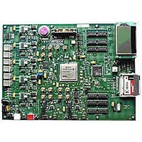
EVALUATION PLATFORM VIRTEX-5
Manufacturer
Xilinx Inc
Series
Virtex™-5 LXTr
Type
FPGAr
Datasheet
1.HW-V5-ML550-UNI-G.pdf
(88 pages)
Specifications of HW-V5-ML550-UNI-G
Contents
Development Platform, Power Supply, Loopback Board, CompactFlash Card, software and documentation
Silicon Manufacturer
Xilinx
Features
64M X 8 DDR SDRAM Memory, Six Samtec LVDS Connectors
Kit Contents
Board, Cable, PSU, CD, Docs
Silicon Family Name
Virtex-5
Silicon Core Number
XC5VLX50T-FFG1136
Rohs Compliant
Yes
Lead Free Status / RoHS Status
Lead free / RoHS Compliant
For Use With/related Products
Virtex™-5 LXT
Lead Free Status / RoHS Status
Lead free / RoHS Compliant, Lead free / RoHS Compliant
Available stocks
Company
Part Number
Manufacturer
Quantity
Price


Chapter 3: Hardware Description
LVDS Connectors
28
2
3
1
4
USB_D-
USB_VBUS
GND
USB_D+
Transmit LVDS
Receive LVDS
5
8
3
4
A high-level block diagram of the USB interface is shown in
cable included in the kit mates with the J22 connector.
The ML550 Development Board provides 53 pairs of transmit signals and 53 pairs of
receive LVDS signals. These signals are distributed across three Samtec QSE-DP connectors
for transmitting and another three connectors for receiving.
pinouts.
The LVDS transmit connectors are shown on schematic pages 6 (TX1, P73, U9 bank 17),
7 (TX2, P46, U9 bank 21) and 8 (TX3, P49, U9 bank 22).
ML550 schematic 0381218 sheet 7 shows FPGA U9.AJ26/AJ25 FPGA_CLKP/N from the
FPGA driving a clock multiplier device U16 detailed on sheet 12. On sheet 12, the U16
ICS8745B clock multiplier is configured in clock-doubler mode. U16 receives the
FPGA_CLKP/N clock waveform on it’s input pins U16.1 and U16.2, and outputs a
doubled frequency on pins U16.13 and U16.12, XMITCLK_P and XMITCLK_N
respectively. This doubled output clock is wired to a Samtec LVDS transmit connector P46,
pins P46.40 and P46.38, on sheet 7.
The LVDS receive connectors are shown on schematic pages 9 (RX1, P74, U9 bank 15), 10
(RX2, P6, U9 bank 19) and 11 (RX3, P3, U9 bank 20).
Each FPGA U9 bank V
interface is LVDS_25.
ML550 schematic 0381218 sheet 10 shows FPGA U9.E28/F28 DIVCLKP/N driven from a
clock divider device U17 detailed on sheet 12. On sheet 12, the U17 On Semi NB6N239S
clock divider is configured in divide-by-2 mode. U17 receives the clock waveform from the
Samtec LVDS receive connector P6 pins P6.47 and P6.49, on sheet 10. This RCVCLK_P and
RCVCLK_N clock waveform drives U17 input pins U17.2 and U17.3 respectively. U17 then
CP2102
U2
Figure 3-6: USB Interface Block Diagram
28
27
26
25
24
23
9
12
USB_DTR_I_B
USB_DSR_I_B
USB_TX_O
USB_RX_I
USB_RTS_O_B
USB_CTS_I_B
USB_RESET_I_B
USB_SUSPEND_O
CCO
www.xilinx.com
is 2.5V, and the intended signalling standard for the LVDS
7
3
8
4
9
5
1
6
MAX3008
U20
ML550 Networking Interfaces Platform
14
18
13
17
12
16
20
15
Appendix A, “LVDS,”
USB_DTR_B
USB_DSR_B
USB_TX
USB_RX
USB_RTS_B
USB_CTS_B
USB_RESET_B
USB_SUSPEND
Figure
UG202 (v1.4) April 18, 2008
3-6. The USB B-to-A
C33
D34
C34
D32
C32
B33
A33
B32
UG202_3_06_050806
Virtex-5
FPGA
lists the
U9
R
Related parts for HW-V5-ML550-UNI-G
Image
Part Number
Description
Manufacturer
Datasheet
Request
R

Part Number:
Description:
IC CPLD .8K 36MCELL 44-VQFP
Manufacturer:
Xilinx Inc
Datasheet:

Part Number:
Description:
IC CPLD 72MCRCELL 10NS 44VQFP
Manufacturer:
Xilinx Inc
Datasheet:

Part Number:
Description:
IC CPLD 1.6K 72MCELL 64-VQFP
Manufacturer:
Xilinx Inc
Datasheet:

Part Number:
Description:
IC CR-II CPLD 64MCELL 44-VQFP
Manufacturer:
Xilinx Inc
Datasheet:

Part Number:
Description:
IC CPLD 1.6K 72MCELL 100-TQFP
Manufacturer:
Xilinx Inc
Datasheet:

Part Number:
Description:
IC CR-II CPLD 64MCELL 56-BGA
Manufacturer:
Xilinx Inc
Datasheet:

Part Number:
Description:
IC CPLD 72MCRCELL 7.5NS 44VQFP
Manufacturer:
Xilinx Inc
Datasheet:
Part Number:
Description:
IC CR-II CPLD 64MCELL 100-VQFP
Manufacturer:
Xilinx Inc
Datasheet:
Part Number:
Description:
IC CPLD 1.6K 72MCELL 100-TQFP
Manufacturer:
Xilinx Inc
Datasheet:

Part Number:
Description:
IC CPLD 72MCRCELL 7.5NS 64VQFP
Manufacturer:
Xilinx Inc
Datasheet:
Part Number:
Description:
IC CPLD 1.6K 72MCELL 100-TQFP
Manufacturer:
Xilinx Inc
Datasheet:

Part Number:
Description:
IC CPLD 1.5K 64MCELL HP 44-VQFP
Manufacturer:
Xilinx Inc

Part Number:
Description:
IC CPLD 36MCRCELL 15NS 44PLCC
Manufacturer:
Xilinx Inc
Datasheet:

Part Number:
Description:
IC CPLD 36MCRCELL 10NS 44PLCC
Manufacturer:
Xilinx Inc
Datasheet:

Part Number:
Description:
IC CPLD 1.5K 64MCELL HP 44-VQFP
Manufacturer:
Xilinx Inc