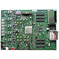
HW-V5-ML550-UNI-G Xilinx Inc, HW-V5-ML550-UNI-G Datasheet - Page 32

HW-V5-ML550-UNI-G
Manufacturer Part Number
HW-V5-ML550-UNI-G
Description
EVALUATION PLATFORM VIRTEX-5
Manufacturer
Xilinx Inc
Series
Virtex™-5 LXTr
Type
FPGAr
Datasheet
1.HW-V5-ML550-UNI-G.pdf
(88 pages)
Specifications of HW-V5-ML550-UNI-G
Contents
Development Platform, Power Supply, Loopback Board, CompactFlash Card, software and documentation
Silicon Manufacturer
Xilinx
Features
64M X 8 DDR SDRAM Memory, Six Samtec LVDS Connectors
Kit Contents
Board, Cable, PSU, CD, Docs
Silicon Family Name
Virtex-5
Silicon Core Number
XC5VLX50T-FFG1136
Rohs Compliant
Yes
Lead Free Status / RoHS Status
Lead free / RoHS Compliant
For Use With/related Products
Virtex™-5 LXT
Lead Free Status / RoHS Status
Lead free / RoHS Compliant, Lead free / RoHS Compliant
Available stocks
Company
Part Number
Manufacturer
Quantity
Price
Chapter 3: Hardware Description
Power Monitor Connector
32
Margin Control
Data Latch
VR_SEL0
VR_SEL1
VR_SEL2
VR_SEL3
STB_VCCINT1V0
FPGA_RESETB
12
13
D
4
5
9
1
8
SN74LV175AD
1D
2D
3D
4D
CLK
CLR
GND
U25
To activate the margin control circuitry FPGA_RESETB is driven High, the desired margin
resistor select data is setup on the VR_SEL[3:0] bus, and the data latch of the voltage
regulator of interest is strobed to capture the resistor select data. See
Strobes
selection of the appropriate R
the selected margin voltage value.
Each regulator has a two-pin test point connector associated with it (pin 1 = V
2 = GND). To apply V
first disable the on-board voltage regulator using the inhibit jumper shown in
and then connect a bench-top power supply to the two-pin test point connector for that
voltage. This provides bench-top power to the power plane and also “back powers” the
output pin of the inhibited voltage regulator.
Note:
supply is ON and attached to the board in the manner described above. The voltage regulator can be
damaged if the output is reverse powered and the 5V input is removed. Always turn the bench-top
power supply OFF first, then turn the 5V power to the ML550 Development Board OFF.
Not shown in
Each voltage regulator is routed to its own 10 m 1% 3W Kelvin current sense resistor. The
V
1Q
2Q
3Q
4Q
1Q
2Q
3Q
4Q
CC
16
2
7
10
15
3
6
11
14
Do not turn OFF the 5V power to the ML550 Development Board while a bench-top power
V
in
CC
Figure 3-9: Margin Control Circuit Details
Table
Figure 3-8
3-9. The latch output drives the analog mux switch select lines to cause
-10%
D
OUT
-7.5%
or
www.xilinx.com
values other than the fixed set the voltage regulator can supply,
Figure 3-9
ADJ
V
-5%
CC
resistor, which causes the regulator to adjust its output to
V
CC
-2.5%
RNom = 84.5 K
is the voltage plane current measurement resistor.
3
1
2
16
15
14
13
12
11
10
9
GND
IN
V
CC
MAX4781EUE
V
X2
X1
X0
X3
A
B
C
MAX4625
V
CC
ADJ
U5
COM
EN_8
GND
ND
NC
U26
NC
X4
X6
X7
X5
X
4
6
5
1
2
3
4
5
6
7
8
ML550 Networking Interfaces Platform
D
+2.5%
UG202 (v1.4) April 18, 2008
2:1 Mux
8:1 Mux
+5%
Margin Control
R
NOM
+7.5%
ug202_3_11_031406
OUT
Figure
+10%
and pin
3-8,
R


