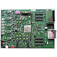
HW-V5-ML550-UNI-G Xilinx Inc, HW-V5-ML550-UNI-G Datasheet - Page 76
HW-V5-ML550-UNI-G
Manufacturer Part Number
HW-V5-ML550-UNI-G
Description
EVALUATION PLATFORM VIRTEX-5
Manufacturer
Xilinx Inc
Series
Virtex™-5 LXTr
Type
FPGAr
Datasheet
1.HW-V5-ML550-UNI-G.pdf
(88 pages)
Specifications of HW-V5-ML550-UNI-G
Contents
Development Platform, Power Supply, Loopback Board, CompactFlash Card, software and documentation
Silicon Manufacturer
Xilinx
Features
64M X 8 DDR SDRAM Memory, Six Samtec LVDS Connectors
Kit Contents
Board, Cable, PSU, CD, Docs
Silicon Family Name
Virtex-5
Silicon Core Number
XC5VLX50T-FFG1136
Rohs Compliant
Yes
Lead Free Status / RoHS Status
Lead free / RoHS Compliant
For Use With/related Products
Virtex™-5 LXT
Lead Free Status / RoHS Status
Lead free / RoHS Compliant, Lead free / RoHS Compliant
Available stocks
Company
Part Number
Manufacturer
Quantity
Price


Appendix C: LCD Interface
Table C-7: Display Instructions
76
8-bit data specified by the column and page address can be read from the Display Data RAM. The column address is increased automatically,
thus data can be read continuously from the addressed page.
8-bit data can be written into a RAM location specified by the column and page address. The column address is increased automatically, thus
data can be written continuously to the addressed page.
BUSY: Device is BUSY when internal operation or reset. (0=active, 1 =busy).
ADC: Indicates the relationship between RAM column address and segment driver.
ONOFF: Indicates display ON or OFF status.
RESETB: Indicates if initialization is in progress.
Turn display ON or OFF. (1=ON, 0 = OFF)
Sets the line address of the display RAM to determine the initial line of the LCD display.
This is a two-byte instruction. The first instruction sets the reference voltage mode. The second instruction sets the reference voltage parameter.
Set reference voltage register
Set reference voltage mode
Write display data
Initial display line
Read display data
Display ON/OFF
Instruction
Read status
Instruction Set
Table C-7
RS
1
1
0
0
0
0
0
ST5
RW
shows the instruction set for the LCD panel.
1
0
1
0
0
0
0
..
1
1
0
0
BUSY
DB7
ST4
SV5
x
1
0
0
0
..
1
1
1
0
0
..
1
1
www.xilinx.com
ADC
DB6
SV4
ST3
0
1
0
0
..
1
1
0
x
0
0
..
1
1
ONOFF
DB5
SV5
SV3
ST5
ST2
1
0
0
..
1
1
0
0
0
..
1
1
RESETB
DB4
ST4
ST1
SV4
SV2
0
0
0
..
1
1
0
0
0
..
1
1
Write Data
Read Data
ML550 Networking Interfaces Platform
DB3
SV3
SV1
ST3
ST0
0
1
0
1
..
0
1
0
0
0
..
1
1
UG202 (v1.4) April 18, 2008
DB2
SV2
SV0
ST2
Line address 62
Line address 63
Line address 0
Line address 1
0
1
0
0
1
..
0
1
..
DB1
SV1
ST1
62
63
0
1
0
0
1
..
DON
DB0
SV0
ST0
0
1
R
Related parts for HW-V5-ML550-UNI-G
Image
Part Number
Description
Manufacturer
Datasheet
Request
R

Part Number:
Description:
IC CPLD .8K 36MCELL 44-VQFP
Manufacturer:
Xilinx Inc
Datasheet:

Part Number:
Description:
IC CPLD 72MCRCELL 10NS 44VQFP
Manufacturer:
Xilinx Inc
Datasheet:

Part Number:
Description:
IC CPLD 1.6K 72MCELL 64-VQFP
Manufacturer:
Xilinx Inc
Datasheet:

Part Number:
Description:
IC CR-II CPLD 64MCELL 44-VQFP
Manufacturer:
Xilinx Inc
Datasheet:

Part Number:
Description:
IC CPLD 1.6K 72MCELL 100-TQFP
Manufacturer:
Xilinx Inc
Datasheet:

Part Number:
Description:
IC CR-II CPLD 64MCELL 56-BGA
Manufacturer:
Xilinx Inc
Datasheet:

Part Number:
Description:
IC CPLD 72MCRCELL 7.5NS 44VQFP
Manufacturer:
Xilinx Inc
Datasheet:
Part Number:
Description:
IC CR-II CPLD 64MCELL 100-VQFP
Manufacturer:
Xilinx Inc
Datasheet:
Part Number:
Description:
IC CPLD 1.6K 72MCELL 100-TQFP
Manufacturer:
Xilinx Inc
Datasheet:

Part Number:
Description:
IC CPLD 72MCRCELL 7.5NS 64VQFP
Manufacturer:
Xilinx Inc
Datasheet:
Part Number:
Description:
IC CPLD 1.6K 72MCELL 100-TQFP
Manufacturer:
Xilinx Inc
Datasheet:

Part Number:
Description:
IC CPLD 1.5K 64MCELL HP 44-VQFP
Manufacturer:
Xilinx Inc

Part Number:
Description:
IC CPLD 36MCRCELL 15NS 44PLCC
Manufacturer:
Xilinx Inc
Datasheet:

Part Number:
Description:
IC CPLD 36MCRCELL 10NS 44PLCC
Manufacturer:
Xilinx Inc
Datasheet:

Part Number:
Description:
IC CPLD 1.5K 64MCELL HP 44-VQFP
Manufacturer:
Xilinx Inc