C8051F996DK Silicon Laboratories Inc, C8051F996DK Datasheet - Page 93
C8051F996DK
Manufacturer Part Number
C8051F996DK
Description
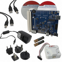
KIT DEV FOR C8051F996
Manufacturer
Silicon Laboratories Inc
Type
MCUr
Datasheets
1.C8051F996DK.pdf
(24 pages)
2.C8051F996DK.pdf
(2 pages)
3.C8051F996DK.pdf
(4 pages)
4.C8051F996DK.pdf
(322 pages)
Specifications of C8051F996DK
Contents
Board, Batteries, Cables, CDs, Debug Adapter, Documentation, Power Adapter
Processor To Be Evaluated
C8051F996
Processor Series
C8051F98x
Interface Type
USB
Operating Supply Voltage
3 V
Lead Free Status / RoHS Status
Lead free / RoHS Compliant
For Use With/related Products
C8051F996
Lead Free Status / Rohs Status
Lead free / RoHS Compliant
Other names
336-1963


7.5.
The SFRs used to enable and configure the comparator are described in the following register
descriptions. The comparator must be enabled by setting the CP0EN bit to logic 1 before it can be used.
From an enabled state, a comparator can be disabled and placed in a low power state by clearing the
CP0EN bit to logic 0.
Important Note About Comparator Settings: False rising and falling edges can be detected by the
Comparator while powering on or if changes are made to the hysteresis or response time control bits.
Therefore, it is recommended that the rising-edge and falling-edge flags be explicitly cleared to logic 0 a
short time after the comparator is enabled or its mode bits have been changed. The Comparator Power Up
Time is specified in Section “Table 4.14. Comparator Electrical Characteristics” on page 61.
(Programmed with CP0HYP Bits)
Comparator Register Descriptions
Positive Hysteresis Voltage
INPUTS
OUTPUT
VIN+
VIN-
CIRCUIT CONFIGURATION
Positive Hysteresis
CP0-
VIN+
CP0+
VIN-
Disabled
V
OL
V
OH
+
_
Figure 7.2. Comparator Hysteresis Plot
CP0
Positive Hysteresis
Maximum
OUT
Rev. 1.0
Negative Hysteresis
Disabled
C8051F99x-C8051F98x
Negative Hysteresis
(Programmed by CP0HYN Bits)
Maximum
Negative Hysteresis Voltage
93
Related parts for C8051F996DK
Image
Part Number
Description
Manufacturer
Datasheet
Request
R

Part Number:
Description:
SMD/C°/SINGLE-ENDED OUTPUT SILICON OSCILLATOR
Manufacturer:
Silicon Laboratories Inc
Part Number:
Description:
Manufacturer:
Silicon Laboratories Inc
Datasheet:
Part Number:
Description:
N/A N/A/SI4010 AES KEYFOB DEMO WITH LCD RX
Manufacturer:
Silicon Laboratories Inc
Datasheet:
Part Number:
Description:
N/A N/A/SI4010 SIMPLIFIED KEY FOB DEMO WITH LED RX
Manufacturer:
Silicon Laboratories Inc
Datasheet:
Part Number:
Description:
N/A/-40 TO 85 OC/EZLINK MODULE; F930/4432 HIGH BAND (REV E/B1)
Manufacturer:
Silicon Laboratories Inc
Part Number:
Description:
EZLink Module; F930/4432 Low Band (rev e/B1)
Manufacturer:
Silicon Laboratories Inc
Part Number:
Description:
I°/4460 10 DBM RADIO TEST CARD 434 MHZ
Manufacturer:
Silicon Laboratories Inc
Part Number:
Description:
I°/4461 14 DBM RADIO TEST CARD 868 MHZ
Manufacturer:
Silicon Laboratories Inc
Part Number:
Description:
I°/4463 20 DBM RFSWITCH RADIO TEST CARD 460 MHZ
Manufacturer:
Silicon Laboratories Inc
Part Number:
Description:
I°/4463 20 DBM RADIO TEST CARD 868 MHZ
Manufacturer:
Silicon Laboratories Inc
Part Number:
Description:
I°/4463 27 DBM RADIO TEST CARD 868 MHZ
Manufacturer:
Silicon Laboratories Inc
Part Number:
Description:
I°/4463 SKYWORKS 30 DBM RADIO TEST CARD 915 MHZ
Manufacturer:
Silicon Laboratories Inc
Part Number:
Description:
N/A N/A/-40 TO 85 OC/4463 RFMD 30 DBM RADIO TEST CARD 915 MHZ
Manufacturer:
Silicon Laboratories Inc
Part Number:
Description:
I°/4463 20 DBM RADIO TEST CARD 169 MHZ
Manufacturer:
Silicon Laboratories Inc