C8051F996DK Silicon Laboratories Inc, C8051F996DK Datasheet - Page 26
C8051F996DK
Manufacturer Part Number
C8051F996DK
Description
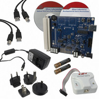
KIT DEV FOR C8051F996
Manufacturer
Silicon Laboratories Inc
Type
MCUr
Datasheets
1.C8051F996DK.pdf
(24 pages)
2.C8051F996DK.pdf
(2 pages)
3.C8051F996DK.pdf
(4 pages)
4.C8051F996DK.pdf
(322 pages)
Specifications of C8051F996DK
Contents
Board, Batteries, Cables, CDs, Debug Adapter, Documentation, Power Adapter
Processor To Be Evaluated
C8051F996
Processor Series
C8051F98x
Interface Type
USB
Operating Supply Voltage
3 V
Lead Free Status / RoHS Status
Lead free / RoHS Compliant
For Use With/related Products
C8051F996
Lead Free Status / Rohs Status
Lead free / RoHS Compliant
Other names
336-1963


C8051F99x-C8051F98x
1.2.
Digital and analog resources are available through 16 or 17 I/O pins. Port pins are organized as three byte-
wide ports. Port pins P0.0–P1.7 can be defined as digital or analog I/O. Digital I/O pins can be assigned to
one of the internal digital resources or used as general purpose I/O (GPIO). Analog I/O pins are used by
the internal analog resources. P2.7 can be used as GPIO and is shared with the C2 Interface Data signal
(C2D). See Section “27. C2 Interface” on page 317 for more details.
The designer has complete control over which digital and analog functions are assigned to individual Port
pins, limited only by the number of physical I/O pins. This resource assignment flexibility is achieved
through the use of a Priority Crossbar Decoder. See Section “21.3. Priority Crossbar Decoder” on
page 217 for more information on the Crossbar.
All Port I/Os can tolerate voltages up to the supply rail when used as digital inputs or open-drain outputs.
For Port I/Os configured as push-pull outputs, current is sourced from the VDD supply. Port I/Os used for
analog functions can operate up to the VDD supply voltage. See Section “21.1. Port I/O Modes of
Operation” on page 214 for more information on Port I/O operating modes and the electrical specifications
chapter for detailed electrical specifications.
26
Highest
Priority
Lowest
Priority
Port Input/Output
SYSCLK
SMBus
Output
T0, T1
UART
P0
P1
P2
SPI0
CP0
PCA
(P0.0-P0.7)
(P1.0-P1.7)
(P2.7)
Figure 1.14. Port I/O Functional Block Diagram
2
4
2
4
4
2
8
8
1
Rev. 1.0
XBR2, PnSKIP
XBR0, XBR1,
Crossbar
Decoder
Registers
Priority
Digital
(ADC0, CP0, and CP1 inputs,
To Analog Peripherals
VREF, IREF0, AGND)
8
8
1
P0MASK, P0MAT
P1MASK, P1MAT
Port Match
Cells
Cells
Cell
I/O
I/O
I/O
P0
P1
P2
PnMDIN Registers
External Interrupts
EX0 and EX1
PnMDOUT,
*P1.5 is not available on
20-pin devices.
P0.0
P0.7
P1.0
P1.7*
P2.7
Related parts for C8051F996DK
Image
Part Number
Description
Manufacturer
Datasheet
Request
R

Part Number:
Description:
SMD/C°/SINGLE-ENDED OUTPUT SILICON OSCILLATOR
Manufacturer:
Silicon Laboratories Inc
Part Number:
Description:
Manufacturer:
Silicon Laboratories Inc
Datasheet:
Part Number:
Description:
N/A N/A/SI4010 AES KEYFOB DEMO WITH LCD RX
Manufacturer:
Silicon Laboratories Inc
Datasheet:
Part Number:
Description:
N/A N/A/SI4010 SIMPLIFIED KEY FOB DEMO WITH LED RX
Manufacturer:
Silicon Laboratories Inc
Datasheet:
Part Number:
Description:
N/A/-40 TO 85 OC/EZLINK MODULE; F930/4432 HIGH BAND (REV E/B1)
Manufacturer:
Silicon Laboratories Inc
Part Number:
Description:
EZLink Module; F930/4432 Low Band (rev e/B1)
Manufacturer:
Silicon Laboratories Inc
Part Number:
Description:
I°/4460 10 DBM RADIO TEST CARD 434 MHZ
Manufacturer:
Silicon Laboratories Inc
Part Number:
Description:
I°/4461 14 DBM RADIO TEST CARD 868 MHZ
Manufacturer:
Silicon Laboratories Inc
Part Number:
Description:
I°/4463 20 DBM RFSWITCH RADIO TEST CARD 460 MHZ
Manufacturer:
Silicon Laboratories Inc
Part Number:
Description:
I°/4463 20 DBM RADIO TEST CARD 868 MHZ
Manufacturer:
Silicon Laboratories Inc
Part Number:
Description:
I°/4463 27 DBM RADIO TEST CARD 868 MHZ
Manufacturer:
Silicon Laboratories Inc
Part Number:
Description:
I°/4463 SKYWORKS 30 DBM RADIO TEST CARD 915 MHZ
Manufacturer:
Silicon Laboratories Inc
Part Number:
Description:
N/A N/A/-40 TO 85 OC/4463 RFMD 30 DBM RADIO TEST CARD 915 MHZ
Manufacturer:
Silicon Laboratories Inc
Part Number:
Description:
I°/4463 20 DBM RADIO TEST CARD 169 MHZ
Manufacturer:
Silicon Laboratories Inc