C8051F996DK Silicon Laboratories Inc, C8051F996DK Datasheet - Page 123
C8051F996DK
Manufacturer Part Number
C8051F996DK
Description
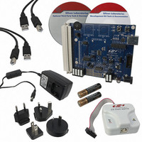
KIT DEV FOR C8051F996
Manufacturer
Silicon Laboratories Inc
Type
MCUr
Datasheets
1.C8051F996DK.pdf
(24 pages)
2.C8051F996DK.pdf
(2 pages)
3.C8051F996DK.pdf
(4 pages)
4.C8051F996DK.pdf
(322 pages)
Specifications of C8051F996DK
Contents
Board, Batteries, Cables, CDs, Debug Adapter, Documentation, Power Adapter
Processor To Be Evaluated
C8051F996
Processor Series
C8051F98x
Interface Type
USB
Operating Supply Voltage
3 V
Lead Free Status / RoHS Status
Lead free / RoHS Compliant
For Use With/related Products
C8051F996
Lead Free Status / Rohs Status
Lead free / RoHS Compliant
Other names
336-1963


C8051F99x-C8051F98x
Notes on Registers, Operands and Addressing Modes:
Rn—Register R0–R7 of the currently selected register bank.
@Ri—Data RAM location addressed indirectly through R0 or R1.
rel—8-bit, signed (twos complement) offset relative to the first byte of the following instruction. Used by
SJMP and all conditional jumps.
direct—8-bit internal data location’s address. This could be a direct-access Data RAM location
(0x00–0x7F) or an SFR (0x80–0xFF).
#data—8-bit constant
#data16—16-bit constant
bit—Direct-accessed bit in Data RAM or SFR
addr11—11-bit destination address used by ACALL and AJMP. The destination must be within the
same 2 kB page of program memory as the first byte of the following instruction.
addr16—16-bit destination address used by LCALL and LJMP. The destination may be anywhere within
the 8 kB program memory space.
There is one unused opcode (0xA5) that performs the same function as NOP.
All mnemonics copyrighted © Intel Corporation 1980.
Rev. 1.0
123
Related parts for C8051F996DK
Image
Part Number
Description
Manufacturer
Datasheet
Request
R

Part Number:
Description:
SMD/C°/SINGLE-ENDED OUTPUT SILICON OSCILLATOR
Manufacturer:
Silicon Laboratories Inc
Part Number:
Description:
Manufacturer:
Silicon Laboratories Inc
Datasheet:
Part Number:
Description:
N/A N/A/SI4010 AES KEYFOB DEMO WITH LCD RX
Manufacturer:
Silicon Laboratories Inc
Datasheet:
Part Number:
Description:
N/A N/A/SI4010 SIMPLIFIED KEY FOB DEMO WITH LED RX
Manufacturer:
Silicon Laboratories Inc
Datasheet:
Part Number:
Description:
N/A/-40 TO 85 OC/EZLINK MODULE; F930/4432 HIGH BAND (REV E/B1)
Manufacturer:
Silicon Laboratories Inc
Part Number:
Description:
EZLink Module; F930/4432 Low Band (rev e/B1)
Manufacturer:
Silicon Laboratories Inc
Part Number:
Description:
I°/4460 10 DBM RADIO TEST CARD 434 MHZ
Manufacturer:
Silicon Laboratories Inc
Part Number:
Description:
I°/4461 14 DBM RADIO TEST CARD 868 MHZ
Manufacturer:
Silicon Laboratories Inc
Part Number:
Description:
I°/4463 20 DBM RFSWITCH RADIO TEST CARD 460 MHZ
Manufacturer:
Silicon Laboratories Inc
Part Number:
Description:
I°/4463 20 DBM RADIO TEST CARD 868 MHZ
Manufacturer:
Silicon Laboratories Inc
Part Number:
Description:
I°/4463 27 DBM RADIO TEST CARD 868 MHZ
Manufacturer:
Silicon Laboratories Inc
Part Number:
Description:
I°/4463 SKYWORKS 30 DBM RADIO TEST CARD 915 MHZ
Manufacturer:
Silicon Laboratories Inc
Part Number:
Description:
N/A N/A/-40 TO 85 OC/4463 RFMD 30 DBM RADIO TEST CARD 915 MHZ
Manufacturer:
Silicon Laboratories Inc
Part Number:
Description:
I°/4463 20 DBM RADIO TEST CARD 169 MHZ
Manufacturer:
Silicon Laboratories Inc