C8051F996DK Silicon Laboratories Inc, C8051F996DK Datasheet - Page 6
C8051F996DK
Manufacturer Part Number
C8051F996DK
Description
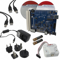
KIT DEV FOR C8051F996
Manufacturer
Silicon Laboratories Inc
Type
MCUr
Datasheets
1.C8051F996DK.pdf
(24 pages)
2.C8051F996DK.pdf
(2 pages)
3.C8051F996DK.pdf
(4 pages)
4.C8051F996DK.pdf
(322 pages)
Specifications of C8051F996DK
Contents
Board, Batteries, Cables, CDs, Debug Adapter, Documentation, Power Adapter
Processor To Be Evaluated
C8051F996
Processor Series
C8051F98x
Interface Type
USB
Operating Supply Voltage
3 V
Lead Free Status / RoHS Status
Lead free / RoHS Compliant
For Use With/related Products
C8051F996
Lead Free Status / Rohs Status
Lead free / RoHS Compliant
Other names
336-1963


C8051F99x-C8051F98x
23. UART0.................................................................................................................... 255
24. Enhanced Serial Peripheral Interface (SPI0)...................................................... 263
25. Timers.................................................................................................................... 276
6
22.3.SMBus Operation ........................................................................................... 235
22.4.Using the SMBus............................................................................................ 237
22.5.SMBus Transfer Modes.................................................................................. 247
22.6.SMBus Status Decoding................................................................................. 250
23.1.Enhanced Baud Rate Generation................................................................... 256
23.2.Operational Modes ......................................................................................... 257
23.3.Multiprocessor Communications .................................................................... 258
24.1.Signal Descriptions......................................................................................... 264
24.2.SPI0 Master Mode Operation ......................................................................... 264
24.3.SPI0 Slave Mode Operation ........................................................................... 266
24.4.SPI0 Interrupt Sources ................................................................................... 267
24.5.Serial Clock Phase and Polarity ..................................................................... 267
24.6.SPI Special Function Registers ...................................................................... 269
25.1.Timer 0 and Timer 1 ....................................................................................... 278
25.2.Timer 2 .......................................................................................................... 286
25.3.Timer 3 .......................................................................................................... 292
22.3.1.Transmitter vs. Receiver ........................................................................ 235
22.3.2.Arbitration............................................................................................... 235
22.3.3.Clock Low Extension.............................................................................. 236
22.3.4.SCL Low Timeout................................................................................... 236
22.3.5.SCL High (SMBus Free) Timeout .......................................................... 236
22.4.1.SMBus Configuration Register............................................................... 238
22.4.2.SMB0CN Control Register ..................................................................... 241
22.4.3.Hardware Slave Address Recognition ................................................... 244
22.4.4.Data Register ......................................................................................... 246
22.5.1.Write Sequence (Master) ....................................................................... 247
22.5.2.Read Sequence (Master) ....................................................................... 248
22.5.3.Write Sequence (Slave) ......................................................................... 249
22.5.4.Read Sequence (Slave) ......................................................................... 250
23.2.1.8-Bit UART ............................................................................................. 257
23.2.2.9-Bit UART ............................................................................................. 258
24.1.1.Master Out, Slave In (MOSI).................................................................. 264
24.1.2.Master In, Slave Out (MISO).................................................................. 264
24.1.3.Serial Clock (SCK) ................................................................................. 264
24.1.4.Slave Select (NSS) ................................................................................ 264
25.1.1.Mode 0: 13-bit Counter/Timer ................................................................ 278
25.1.2.Mode 1: 16-bit Counter/Timer ................................................................ 279
25.1.3.Mode 2: 8-bit Counter/Timer with Auto-Reload...................................... 280
25.1.4.Mode 3: Two 8-bit Counter/Timers (Timer 0 Only)................................. 281
25.2.1.16-bit Timer with Auto-Reload................................................................ 286
25.2.2.8-bit Timers with Auto-Reload................................................................ 287
25.2.3.Comparator 0/SmaRTClock Capture Mode ........................................... 288
Rev. 1.0
Related parts for C8051F996DK
Image
Part Number
Description
Manufacturer
Datasheet
Request
R

Part Number:
Description:
SMD/C°/SINGLE-ENDED OUTPUT SILICON OSCILLATOR
Manufacturer:
Silicon Laboratories Inc
Part Number:
Description:
Manufacturer:
Silicon Laboratories Inc
Datasheet:
Part Number:
Description:
N/A N/A/SI4010 AES KEYFOB DEMO WITH LCD RX
Manufacturer:
Silicon Laboratories Inc
Datasheet:
Part Number:
Description:
N/A N/A/SI4010 SIMPLIFIED KEY FOB DEMO WITH LED RX
Manufacturer:
Silicon Laboratories Inc
Datasheet:
Part Number:
Description:
N/A/-40 TO 85 OC/EZLINK MODULE; F930/4432 HIGH BAND (REV E/B1)
Manufacturer:
Silicon Laboratories Inc
Part Number:
Description:
EZLink Module; F930/4432 Low Band (rev e/B1)
Manufacturer:
Silicon Laboratories Inc
Part Number:
Description:
I°/4460 10 DBM RADIO TEST CARD 434 MHZ
Manufacturer:
Silicon Laboratories Inc
Part Number:
Description:
I°/4461 14 DBM RADIO TEST CARD 868 MHZ
Manufacturer:
Silicon Laboratories Inc
Part Number:
Description:
I°/4463 20 DBM RFSWITCH RADIO TEST CARD 460 MHZ
Manufacturer:
Silicon Laboratories Inc
Part Number:
Description:
I°/4463 20 DBM RADIO TEST CARD 868 MHZ
Manufacturer:
Silicon Laboratories Inc
Part Number:
Description:
I°/4463 27 DBM RADIO TEST CARD 868 MHZ
Manufacturer:
Silicon Laboratories Inc
Part Number:
Description:
I°/4463 SKYWORKS 30 DBM RADIO TEST CARD 915 MHZ
Manufacturer:
Silicon Laboratories Inc
Part Number:
Description:
N/A N/A/-40 TO 85 OC/4463 RFMD 30 DBM RADIO TEST CARD 915 MHZ
Manufacturer:
Silicon Laboratories Inc
Part Number:
Description:
I°/4463 20 DBM RADIO TEST CARD 169 MHZ
Manufacturer:
Silicon Laboratories Inc