C8051F996DK Silicon Laboratories Inc, C8051F996DK Datasheet - Page 75
C8051F996DK
Manufacturer Part Number
C8051F996DK
Description
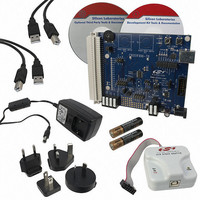
KIT DEV FOR C8051F996
Manufacturer
Silicon Laboratories Inc
Type
MCUr
Datasheets
1.C8051F996DK.pdf
(24 pages)
2.C8051F996DK.pdf
(2 pages)
3.C8051F996DK.pdf
(4 pages)
4.C8051F996DK.pdf
(322 pages)
Specifications of C8051F996DK
Contents
Board, Batteries, Cables, CDs, Debug Adapter, Documentation, Power Adapter
Processor To Be Evaluated
C8051F996
Processor Series
C8051F98x
Interface Type
USB
Operating Supply Voltage
3 V
Lead Free Status / RoHS Status
Lead free / RoHS Compliant
For Use With/related Products
C8051F996
Lead Free Status / Rohs Status
Lead free / RoHS Compliant
Other names
336-1963


SFR Definition 5.4. ADC0PWR: ADC0 Burst Mode Power-Up Time
SFR Page = All; SFR Address = 0xBB
Name
Reset
Bit
Type
6:4
3:0
7
Bit
AD0PWR[3:0] ADC0 Burst Mode Power-Up Time.
AD0LPM
AD0LPM
Unused
Name
R/W
7
0
ADC0 Low Power Mode Enable.
Enables Low Power Mode Operation.
0: Low Power Mode disabled.
1: Low Power Mode enabled.
Read = 0000b; Write = Don’t Care.
Sets the time delay required for ADC0 to power up from a low power state.
For BURSTEN = 0:
For BURSTEN = 1 and AD0EN = 1:
all conversions are complete.
Conversions can begin immediately following the start-of-conversion signal.
For BURSTEN = 1 and AD0EN = 0:
Conversions can begin a programmed delay after the start-of-conversion signal.
The ADC0 Burst Mode Power-Up time is programmed according to the following
equation:
Note: Setting AD0PWR to 0x04 provides a typical tracking time of 2 us for the first sample
R
6
0
or
AD0PWR
Tstartup
taken after the start of conversion.
R
5
0
=
=
ADC0 power state controlled by AD0EN.
ADC0 remains enabled and does not enter a low power state after
ADC0 enters a low power state after all conversions are complete.
Tstartup
---------------------- 1
AD0PWR
400ns
Rev. 1.0
R
4
0
–
+
1
C8051F99x-C8051F98x
400ns
Function
3
1
AD0PWR[3:0]
2
1
R/W
1
1
0
1
75
Related parts for C8051F996DK
Image
Part Number
Description
Manufacturer
Datasheet
Request
R

Part Number:
Description:
SMD/C°/SINGLE-ENDED OUTPUT SILICON OSCILLATOR
Manufacturer:
Silicon Laboratories Inc
Part Number:
Description:
Manufacturer:
Silicon Laboratories Inc
Datasheet:
Part Number:
Description:
N/A N/A/SI4010 AES KEYFOB DEMO WITH LCD RX
Manufacturer:
Silicon Laboratories Inc
Datasheet:
Part Number:
Description:
N/A N/A/SI4010 SIMPLIFIED KEY FOB DEMO WITH LED RX
Manufacturer:
Silicon Laboratories Inc
Datasheet:
Part Number:
Description:
N/A/-40 TO 85 OC/EZLINK MODULE; F930/4432 HIGH BAND (REV E/B1)
Manufacturer:
Silicon Laboratories Inc
Part Number:
Description:
EZLink Module; F930/4432 Low Band (rev e/B1)
Manufacturer:
Silicon Laboratories Inc
Part Number:
Description:
I°/4460 10 DBM RADIO TEST CARD 434 MHZ
Manufacturer:
Silicon Laboratories Inc
Part Number:
Description:
I°/4461 14 DBM RADIO TEST CARD 868 MHZ
Manufacturer:
Silicon Laboratories Inc
Part Number:
Description:
I°/4463 20 DBM RFSWITCH RADIO TEST CARD 460 MHZ
Manufacturer:
Silicon Laboratories Inc
Part Number:
Description:
I°/4463 20 DBM RADIO TEST CARD 868 MHZ
Manufacturer:
Silicon Laboratories Inc
Part Number:
Description:
I°/4463 27 DBM RADIO TEST CARD 868 MHZ
Manufacturer:
Silicon Laboratories Inc
Part Number:
Description:
I°/4463 SKYWORKS 30 DBM RADIO TEST CARD 915 MHZ
Manufacturer:
Silicon Laboratories Inc
Part Number:
Description:
N/A N/A/-40 TO 85 OC/4463 RFMD 30 DBM RADIO TEST CARD 915 MHZ
Manufacturer:
Silicon Laboratories Inc
Part Number:
Description:
I°/4463 20 DBM RADIO TEST CARD 169 MHZ
Manufacturer:
Silicon Laboratories Inc