C8051F996DK Silicon Laboratories Inc, C8051F996DK Datasheet - Page 160
C8051F996DK
Manufacturer Part Number
C8051F996DK
Description
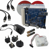
KIT DEV FOR C8051F996
Manufacturer
Silicon Laboratories Inc
Type
MCUr
Datasheets
1.C8051F996DK.pdf
(24 pages)
2.C8051F996DK.pdf
(2 pages)
3.C8051F996DK.pdf
(4 pages)
4.C8051F996DK.pdf
(322 pages)
Specifications of C8051F996DK
Contents
Board, Batteries, Cables, CDs, Debug Adapter, Documentation, Power Adapter
Processor To Be Evaluated
C8051F996
Processor Series
C8051F98x
Interface Type
USB
Operating Supply Voltage
3 V
Lead Free Status / RoHS Status
Lead free / RoHS Compliant
For Use With/related Products
C8051F996
Lead Free Status / Rohs Status
Lead free / RoHS Compliant
Other names
336-1963


C8051F99x-C8051F98x
SFR Definition 14.5. FLSCL: Flash Scale
SFR Page = All; SFR Address = 0xB7
SFR Definition 14.6. FLWR: Flash Write Only
SFR Page = All; SFR Address = 0xE5
160
Note: Operations which clear the BYPASS bit do not need to be immediately followed by a benign 3-byte instruction.
Name
Reset
Name
Reset
Bit
5:0
Bit
7:0
Type
Type
7
6
Bit
Bit
For code compatibility with C8051F930/31/20/21 devices, a benign 3-byte instruction whose third byte is a
don't care should follow the clear operation. See the C8051F93x-C8051F92x data sheet for more details.
FLWR[7:0] Flash Write Only.
Reserved
Reserved
BYPASS
Name
Name
R
7
0
7
0
Always Write to 0.
Flash Read Timing One-Shot Bypass.
0: The one-shot determines the Flash read time. This setting should be used for oper-
ating frequencies less than 14 MHz.
1: The system clock determines the Flash read time. This setting should be used for
frequencies greater than 14 MHz.
Reserved. Always Write to 000000.
All writes to this register have no effect on system operation.
BYPASS
R/W
6
0
6
0
R
5
0
5
0
Rev. 1.0
R
4
0
4
0
FLWR[7:0]
W
Function
Function
R
3
0
3
0
R
2
0
2
0
R
1
0
1
0
R
0
0
0
0
Related parts for C8051F996DK
Image
Part Number
Description
Manufacturer
Datasheet
Request
R

Part Number:
Description:
SMD/C°/SINGLE-ENDED OUTPUT SILICON OSCILLATOR
Manufacturer:
Silicon Laboratories Inc
Part Number:
Description:
Manufacturer:
Silicon Laboratories Inc
Datasheet:
Part Number:
Description:
N/A N/A/SI4010 AES KEYFOB DEMO WITH LCD RX
Manufacturer:
Silicon Laboratories Inc
Datasheet:
Part Number:
Description:
N/A N/A/SI4010 SIMPLIFIED KEY FOB DEMO WITH LED RX
Manufacturer:
Silicon Laboratories Inc
Datasheet:
Part Number:
Description:
N/A/-40 TO 85 OC/EZLINK MODULE; F930/4432 HIGH BAND (REV E/B1)
Manufacturer:
Silicon Laboratories Inc
Part Number:
Description:
EZLink Module; F930/4432 Low Band (rev e/B1)
Manufacturer:
Silicon Laboratories Inc
Part Number:
Description:
I°/4460 10 DBM RADIO TEST CARD 434 MHZ
Manufacturer:
Silicon Laboratories Inc
Part Number:
Description:
I°/4461 14 DBM RADIO TEST CARD 868 MHZ
Manufacturer:
Silicon Laboratories Inc
Part Number:
Description:
I°/4463 20 DBM RFSWITCH RADIO TEST CARD 460 MHZ
Manufacturer:
Silicon Laboratories Inc
Part Number:
Description:
I°/4463 20 DBM RADIO TEST CARD 868 MHZ
Manufacturer:
Silicon Laboratories Inc
Part Number:
Description:
I°/4463 27 DBM RADIO TEST CARD 868 MHZ
Manufacturer:
Silicon Laboratories Inc
Part Number:
Description:
I°/4463 SKYWORKS 30 DBM RADIO TEST CARD 915 MHZ
Manufacturer:
Silicon Laboratories Inc
Part Number:
Description:
N/A N/A/-40 TO 85 OC/4463 RFMD 30 DBM RADIO TEST CARD 915 MHZ
Manufacturer:
Silicon Laboratories Inc
Part Number:
Description:
I°/4463 20 DBM RADIO TEST CARD 169 MHZ
Manufacturer:
Silicon Laboratories Inc