C8051F996DK Silicon Laboratories Inc, C8051F996DK Datasheet - Page 4
C8051F996DK
Manufacturer Part Number
C8051F996DK
Description
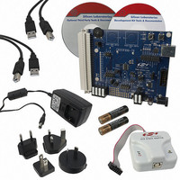
KIT DEV FOR C8051F996
Manufacturer
Silicon Laboratories Inc
Type
MCUr
Datasheets
1.C8051F996DK.pdf
(24 pages)
2.C8051F996DK.pdf
(2 pages)
3.C8051F996DK.pdf
(4 pages)
4.C8051F996DK.pdf
(322 pages)
Specifications of C8051F996DK
Contents
Board, Batteries, Cables, CDs, Debug Adapter, Documentation, Power Adapter
Processor To Be Evaluated
C8051F996
Processor Series
C8051F98x
Interface Type
USB
Operating Supply Voltage
3 V
Lead Free Status / RoHS Status
Lead free / RoHS Compliant
For Use With/related Products
C8051F996
Lead Free Status / Rohs Status
Lead free / RoHS Compliant
Other names
336-1963


C8051F99x-C8051F98x
14. Flash Memory ....................................................................................................... 149
15. Power Management.............................................................................................. 161
16. Cyclic Redundancy Check Unit (CRC0) ............................................................. 170
17. Voltage Regulator (VREG0) ................................................................................. 178
18. Reset Sources....................................................................................................... 179
19. Clocking Sources ................................................................................................. 186
4
13.4.Interrupt Latency............................................................................................. 138
13.5.Interrupt Register Descriptions ....................................................................... 140
13.6.External Interrupts INT0 and INT1.................................................................. 147
14.1.Programming the Flash Memory .................................................................... 149
14.2.Non-volatile Data Storage .............................................................................. 150
14.3.Security Options ............................................................................................. 151
14.4.Determining the Device Part Number at Run Time ........................................ 153
14.5.Flash Write and Erase Guidelines .................................................................. 155
14.6.Minimizing Flash Read Current ...................................................................... 157
15.1.Normal Mode .................................................................................................. 162
15.2.Idle Mode........................................................................................................ 163
15.3.Stop Mode ...................................................................................................... 163
15.4.Suspend Mode ............................................................................................... 164
15.5.Sleep Mode .................................................................................................... 164
15.6.Configuring Wakeup Sources......................................................................... 165
15.7.Determining the Event that Caused the Last Wakeup.................................... 165
15.8.Power Management Specifications ................................................................ 169
16.1.CRC Algorithm................................................................................................ 170
16.2.Preparing for a CRC Calculation .................................................................... 172
16.3.Performing a CRC Calculation ....................................................................... 172
16.4.Accessing the CRC0 Result ........................................................................... 172
16.5.CRC0 Bit Reverse Feature............................................................................. 177
17.1.Voltage Regulator Electrical Specifications .................................................... 178
18.1.Power-On Reset ............................................................................................. 180
18.2.Power-Fail Reset ............................................................................................ 180
18.3.External Reset ................................................................................................ 182
18.4.Missing Clock Detector Reset ........................................................................ 182
18.5.Comparator0 Reset ........................................................................................ 183
18.6.PCA Watchdog Timer Reset .......................................................................... 183
18.7.Flash Error Reset ........................................................................................... 183
18.8.SmaRTClock (Real Time Clock) Reset .......................................................... 183
18.9.Software Reset ............................................................................................... 184
19.1.Programmable Precision Internal Oscillator ................................................... 187
14.1.1.Flash Lock and Key Functions ............................................................... 149
14.1.2.Flash Erase Procedure .......................................................................... 150
14.1.3.Flash Write Procedure ........................................................................... 150
14.5.1.V
14.5.2.PSWE Maintenance ............................................................................... 156
14.5.3.System Clock ......................................................................................... 156
DD
Maintenance and the V
Rev. 1.0
DD
Monitor ................................................. 155
Related parts for C8051F996DK
Image
Part Number
Description
Manufacturer
Datasheet
Request
R

Part Number:
Description:
SMD/C°/SINGLE-ENDED OUTPUT SILICON OSCILLATOR
Manufacturer:
Silicon Laboratories Inc
Part Number:
Description:
Manufacturer:
Silicon Laboratories Inc
Datasheet:
Part Number:
Description:
N/A N/A/SI4010 AES KEYFOB DEMO WITH LCD RX
Manufacturer:
Silicon Laboratories Inc
Datasheet:
Part Number:
Description:
N/A N/A/SI4010 SIMPLIFIED KEY FOB DEMO WITH LED RX
Manufacturer:
Silicon Laboratories Inc
Datasheet:
Part Number:
Description:
N/A/-40 TO 85 OC/EZLINK MODULE; F930/4432 HIGH BAND (REV E/B1)
Manufacturer:
Silicon Laboratories Inc
Part Number:
Description:
EZLink Module; F930/4432 Low Band (rev e/B1)
Manufacturer:
Silicon Laboratories Inc
Part Number:
Description:
I°/4460 10 DBM RADIO TEST CARD 434 MHZ
Manufacturer:
Silicon Laboratories Inc
Part Number:
Description:
I°/4461 14 DBM RADIO TEST CARD 868 MHZ
Manufacturer:
Silicon Laboratories Inc
Part Number:
Description:
I°/4463 20 DBM RFSWITCH RADIO TEST CARD 460 MHZ
Manufacturer:
Silicon Laboratories Inc
Part Number:
Description:
I°/4463 20 DBM RADIO TEST CARD 868 MHZ
Manufacturer:
Silicon Laboratories Inc
Part Number:
Description:
I°/4463 27 DBM RADIO TEST CARD 868 MHZ
Manufacturer:
Silicon Laboratories Inc
Part Number:
Description:
I°/4463 SKYWORKS 30 DBM RADIO TEST CARD 915 MHZ
Manufacturer:
Silicon Laboratories Inc
Part Number:
Description:
N/A N/A/-40 TO 85 OC/4463 RFMD 30 DBM RADIO TEST CARD 915 MHZ
Manufacturer:
Silicon Laboratories Inc
Part Number:
Description:
I°/4463 20 DBM RADIO TEST CARD 169 MHZ
Manufacturer:
Silicon Laboratories Inc