C8051F996DK Silicon Laboratories Inc, C8051F996DK Datasheet - Page 164
C8051F996DK
Manufacturer Part Number
C8051F996DK
Description
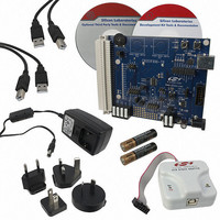
KIT DEV FOR C8051F996
Manufacturer
Silicon Laboratories Inc
Type
MCUr
Datasheets
1.C8051F996DK.pdf
(24 pages)
2.C8051F996DK.pdf
(2 pages)
3.C8051F996DK.pdf
(4 pages)
4.C8051F996DK.pdf
(322 pages)
Specifications of C8051F996DK
Contents
Board, Batteries, Cables, CDs, Debug Adapter, Documentation, Power Adapter
Processor To Be Evaluated
C8051F996
Processor Series
C8051F98x
Interface Type
USB
Operating Supply Voltage
3 V
Lead Free Status / RoHS Status
Lead free / RoHS Compliant
For Use With/related Products
C8051F996
Lead Free Status / Rohs Status
Lead free / RoHS Compliant
Other names
336-1963


C8051F99x-C8051F98x
15.4. Suspend Mode
Setting the Suspend Mode Select bit (PMU0CF.6) causes the system clock to be gated off and all internal
oscillators disabled. The system clock source must be set to the low power internal oscillator or the preci-
sion oscillator prior to entering Suspend Mode. All digital logic (timers, communication peripherals, inter-
rupts, CPU, etc.) stops functioning until one of the enabled wake-up sources occurs.
The following wake-up sources can be configured to wake the device from Suspend Mode:
Note: Upon wake-up from suspend mode, PMU0 requires two system clocks in order to update the PMU0CF wake-
In addition, a noise glitch on RST that is not long enough to reset the device will cause the device to exit
suspend. In order for the MCU to respond to the pin reset event, software must not place the device back
into suspend mode for a period of 15 µs. The PMU0CF register may be checked to determine if the wake-
up was due to a falling edge on the /RST pin. If the wake-up source is not due to a falling edge on RST,
there is no time restriction on how soon software may place the device back into suspend mode. A 4.7 kW
pullup resistor to VDD is recommend for RST to prevent noise glitches from waking the device.
15.5. Sleep Mode
Setting the Sleep Mode Select bit (PMU0CF.7) turns off the internal 1.8 V regulator (VREG0) and switches
the power supply of all on-chip RAM to the VDD pin (see Figure 15.1). Power to most digital logic on the
chip is disconnected; only PMU0 and the SmaRTClock remain powered. Analog peripherals remain pow-
ered in two-cell mode. Only the Comparators remain functional when the device enters Sleep Mode. All
other analog peripherals (CS0, ADC0, IREF0, External Oscillator, etc.) should be disabled prior to entering
Sleep Mode. The system clock source must be set to the low power internal oscillator or the precision
oscillator prior to entering Sleep Mode.
GPIO pins configured as digital outputs will retain their output state during sleep mode. In two-cell mode,
they will maintain the same current drive capability in sleep mode as they have in normal mode.
GPIO pins configured as digital inputs can be used during sleep mode as wakeup sources using the port
match feature. In two-cell mode, they will maintain the same input level specs in sleep mode as they have
in normal mode.
‘C8051F99x-C8051F98x devices support a wakeup request for external devices. Upon exit from sleep
mode, the wake-up request signal is driven low, allowing other devices in the system to wake up from their
low power modes.
RAM and SFR register contents are preserved in sleep mode as long as the voltage on VBAT does not fall
below V
resume code execution upon waking up from sleep mode.
164
CS0 End of Conversion or End of Scan
SmaRTClock Oscillator Fail
SmaRTClock Alarm
Port Match Event
Comparator0 Rising Edge
up flags. All flags will read back a value of '0' during the first two system clocks following a wake-up from
suspend mode.
POR
. The PC counter and all other volatile state information is preserved allowing the device to
Rev. 1.0
Related parts for C8051F996DK
Image
Part Number
Description
Manufacturer
Datasheet
Request
R

Part Number:
Description:
SMD/C°/SINGLE-ENDED OUTPUT SILICON OSCILLATOR
Manufacturer:
Silicon Laboratories Inc
Part Number:
Description:
Manufacturer:
Silicon Laboratories Inc
Datasheet:
Part Number:
Description:
N/A N/A/SI4010 AES KEYFOB DEMO WITH LCD RX
Manufacturer:
Silicon Laboratories Inc
Datasheet:
Part Number:
Description:
N/A N/A/SI4010 SIMPLIFIED KEY FOB DEMO WITH LED RX
Manufacturer:
Silicon Laboratories Inc
Datasheet:
Part Number:
Description:
N/A/-40 TO 85 OC/EZLINK MODULE; F930/4432 HIGH BAND (REV E/B1)
Manufacturer:
Silicon Laboratories Inc
Part Number:
Description:
EZLink Module; F930/4432 Low Band (rev e/B1)
Manufacturer:
Silicon Laboratories Inc
Part Number:
Description:
I°/4460 10 DBM RADIO TEST CARD 434 MHZ
Manufacturer:
Silicon Laboratories Inc
Part Number:
Description:
I°/4461 14 DBM RADIO TEST CARD 868 MHZ
Manufacturer:
Silicon Laboratories Inc
Part Number:
Description:
I°/4463 20 DBM RFSWITCH RADIO TEST CARD 460 MHZ
Manufacturer:
Silicon Laboratories Inc
Part Number:
Description:
I°/4463 20 DBM RADIO TEST CARD 868 MHZ
Manufacturer:
Silicon Laboratories Inc
Part Number:
Description:
I°/4463 27 DBM RADIO TEST CARD 868 MHZ
Manufacturer:
Silicon Laboratories Inc
Part Number:
Description:
I°/4463 SKYWORKS 30 DBM RADIO TEST CARD 915 MHZ
Manufacturer:
Silicon Laboratories Inc
Part Number:
Description:
N/A N/A/-40 TO 85 OC/4463 RFMD 30 DBM RADIO TEST CARD 915 MHZ
Manufacturer:
Silicon Laboratories Inc
Part Number:
Description:
I°/4463 20 DBM RADIO TEST CARD 169 MHZ
Manufacturer:
Silicon Laboratories Inc