C8051F996DK Silicon Laboratories Inc, C8051F996DK Datasheet - Page 215
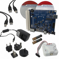
C8051F996DK
Manufacturer Part Number
C8051F996DK
Description
KIT DEV FOR C8051F996
Manufacturer
Silicon Laboratories Inc
Type
MCUr
Datasheets
1.C8051F996DK.pdf
(24 pages)
2.C8051F996DK.pdf
(2 pages)
3.C8051F996DK.pdf
(4 pages)
4.C8051F996DK.pdf
(322 pages)
Specifications of C8051F996DK
Contents
Board, Batteries, Cables, CDs, Debug Adapter, Documentation, Power Adapter
Processor To Be Evaluated
C8051F996
Processor Series
C8051F98x
Interface Type
USB
Operating Supply Voltage
3 V
Lead Free Status / RoHS Status
Lead free / RoHS Compliant
For Use With/related Products
C8051F996
Lead Free Status / Rohs Status
Lead free / RoHS Compliant
Other names
336-1963


21.1.3. Interfacing Port I/O to 5 V Logic
All Port I/O have internal ESD protection diodes to prevent the pin voltage from exceeding the V
The Port I/O pins are not 5V tolerant and require level translators to interface to 5V logic.
21.1.4. Increasing Port I/O Drive Strength
Port I/O output drivers support a high and low drive strength; the default is low drive strength. The drive
strength of a Port I/O can be configured using the PnDRV registers. See Section “4. Electrical Characteris-
tics” on page 46 for the difference in output drive strength between the two modes.
21.2. Assigning Port I/O Pins to Analog and Digital Functions
Port I/O pins P0.0–P1.7 can be assigned to various analog, digital, and external interrupt functions. The
Port pins assuaged to analog functions should be configured for analog I/O and Port pins assuaged to dig-
ital or external interrupt functions should be configured for digital I/O.
21.2.1. Assigning Port I/O Pins to Analog Functions
Table 21.1 shows all available analog functions that need Port I/O assignments. Port pins selected for
these analog functions should have their digital drivers disabled (PnMDOUT.n = 0 and Port Latch =
1) and their corresponding bit in PnSKIP set to 1. This reserves the pin for use by the analog function
and does not allow it to be claimed by the Crossbar. Table 21.1 shows the potential mapping of Port I/O to
each analog function.
Analog Function
ADC Input
Comparator0 Input
Voltage Reference (VREF0)
Analog Ground Reference (AGND)
Current Reference (IREF0)
External Oscillator Input (XTAL1)
External Oscillator Output (XTAL2)
SmaRTClock Oscillator Input (XTAL3)
SmaRTClock Oscillator Output (XTAL4)
Table 21.1. Port I/O Assignment for Analog Functions
Rev. 1.0
Assignable Port Pins
P0.1–P0.7, P1.2–P1.4
Potentially
P1.0, P1.1
C8051F99x-C8051F98x
P0.0
P0.1
P0.7
P0.2
P0.3
P1.6
P1.7
Registers used for
IREF0CN, PnSKIP
OSCXCN, PnSKIP
OSCXCN, PnSKIP
ADC0MX, PnSKIP
CPT0MX, PnSKIP
REF0CN, PnSKIP
REF0CN, PnSKIP
RTC0CN, PnSKIP
RTC0CN, PnSKIP
Assignment
DD
supply.
215
Related parts for C8051F996DK
Image
Part Number
Description
Manufacturer
Datasheet
Request
R

Part Number:
Description:
SMD/C°/SINGLE-ENDED OUTPUT SILICON OSCILLATOR
Manufacturer:
Silicon Laboratories Inc
Part Number:
Description:
Manufacturer:
Silicon Laboratories Inc
Datasheet:
Part Number:
Description:
N/A N/A/SI4010 AES KEYFOB DEMO WITH LCD RX
Manufacturer:
Silicon Laboratories Inc
Datasheet:
Part Number:
Description:
N/A N/A/SI4010 SIMPLIFIED KEY FOB DEMO WITH LED RX
Manufacturer:
Silicon Laboratories Inc
Datasheet:
Part Number:
Description:
N/A/-40 TO 85 OC/EZLINK MODULE; F930/4432 HIGH BAND (REV E/B1)
Manufacturer:
Silicon Laboratories Inc
Part Number:
Description:
EZLink Module; F930/4432 Low Band (rev e/B1)
Manufacturer:
Silicon Laboratories Inc
Part Number:
Description:
I°/4460 10 DBM RADIO TEST CARD 434 MHZ
Manufacturer:
Silicon Laboratories Inc
Part Number:
Description:
I°/4461 14 DBM RADIO TEST CARD 868 MHZ
Manufacturer:
Silicon Laboratories Inc
Part Number:
Description:
I°/4463 20 DBM RFSWITCH RADIO TEST CARD 460 MHZ
Manufacturer:
Silicon Laboratories Inc
Part Number:
Description:
I°/4463 20 DBM RADIO TEST CARD 868 MHZ
Manufacturer:
Silicon Laboratories Inc
Part Number:
Description:
I°/4463 27 DBM RADIO TEST CARD 868 MHZ
Manufacturer:
Silicon Laboratories Inc
Part Number:
Description:
I°/4463 SKYWORKS 30 DBM RADIO TEST CARD 915 MHZ
Manufacturer:
Silicon Laboratories Inc
Part Number:
Description:
N/A N/A/-40 TO 85 OC/4463 RFMD 30 DBM RADIO TEST CARD 915 MHZ
Manufacturer:
Silicon Laboratories Inc
Part Number:
Description:
I°/4463 20 DBM RADIO TEST CARD 169 MHZ
Manufacturer:
Silicon Laboratories Inc