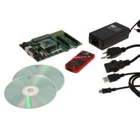
DV164136 Microchip Technology, DV164136 Datasheet - Page 326

DV164136
Manufacturer Part Number
DV164136
Description
DEVELOPMENT KIT FOR PIC18
Manufacturer
Microchip Technology
Series
PIC®r
Type
MCUr
Datasheets
1.DM183032.pdf
(38 pages)
2.DV164136.pdf
(448 pages)
3.DV164136.pdf
(6 pages)
4.DV164136.pdf
(446 pages)
5.DV164136.pdf
(4 pages)
6.DV164136.pdf
(18 pages)
Specifications of DV164136
Contents
Board, Cables, CDs, PICkit™ 3 Programmer, Power Supply
Processor To Be Evaluated
PIC18F8722, PIC18F87J11
Interface Type
RS-232, USB
Operating Supply Voltage
3.3 V, 5 V
Silicon Manufacturer
Microchip
Core Architecture
PIC
Core Sub-architecture
PIC18
Silicon Core Number
PIC18F
Silicon Family Name
PIC18F8xxx
Kit Contents
PIC18 Exp Brd PICkit 3 Cable CD PSU
Lead Free Status / RoHS Status
Lead free / RoHS Compliant
For Use With/related Products
PIC18F8722, PIC18F87J11
Lead Free Status / Rohs Status
Lead free / RoHS Compliant
Available stocks
Company
Part Number
Manufacturer
Quantity
Price
Company:
Part Number:
DV164136
Manufacturer:
MICROCHIP
Quantity:
12 000
- DM183032 PDF datasheet
- DV164136 PDF datasheet #2
- DV164136 PDF datasheet #3
- DV164136 PDF datasheet #4
- DV164136 PDF datasheet #5
- DV164136 PDF datasheet #6
- Current page: 326 of 448
- Download datasheet (8Mb)
PIC18F87J11 FAMILY
24.3.2
When the on-chip regulator is enabled, PIC18F87J11
family devices also have a simple brown-out capability.
If the voltage supplied to the regulator is inadequate to
maintain a regulated level, the regulator Reset circuitry
will generate a Brown-out Reset. This event is captured
by the BOR flag bit (RCON<0>).
The operation of the Brown-out Reset is described in
more detail in Section 4.4 “Brown-out Reset (BOR)”
and Section 4.4.1 “Detecting BOR”. The brown-out
voltage levels are specific in Section 27.1 “DC Char-
acteristics: Supply Voltage PIC18F87J11 Family
(Industrial)”.
24.3.3
The on-chip regulator is designed to meet the power-up
requirements for the device. If the application does not
use the regulator, then strict power-up conditions must
be adhered to. While powering up, V
never exceed V
24.3.4
When enabled, the on-chip regulator always consumes
a small incremental amount of current over I
includes when the device is in Sleep mode, even
though the core digital logic does not require power. To
provide additional savings in applications where power
resources are critical, the regulator can be configured
to automatically disable itself whenever the device
goes into Sleep mode. This feature is controlled by the
REGSLP bit (WDTCON<7>, Register 24-9). Setting
this bit disables the regulator in Sleep mode and
reduces its current consumption to a minimum.
FIGURE 24-3:
DS39778D-page 326
ON-CHIP REGULATOR AND BOR
POWER-UP REQUIREMENTS
OPERATION IN SLEEP MODE
Note 1:
CPU Clock
PLL Clock
Peripheral
Program
Counter
DD
INTRC
Output
OSC1
Clock
by 0.3 volts.
T
OST
TIMING TRANSITION FOR TWO-SPEED START-UP (INTRC TO HSPLL)
Wake from Interrupt Event
= 1024 T
PC
OSC
; T
Q1
PLL
T
OST
= 2 ms (approx). These intervals are not shown to scale.
DDCORE
(1)
Q2
PC + 2
DD
OSTS bit Set
. This
must
T
Q3
PLL
(1)
Q4
Substantial Sleep mode power savings can be obtained
by setting the REGSLP bit, but device wake-up time will
increase in order to insure the regulator has enough time
to stabilize. The REGSLP bit is automatically cleared by
hardware when a Low-Voltage Detect condition occurs.
24.4
The Two-Speed Start-up feature helps to minimize the
latency period, from oscillator start-up to code execu-
tion, by allowing the microcontroller to use the INTRC
oscillator as a clock source until the primary clock
source is available. It is enabled by setting the IESO
Configuration bit.
Two-Speed Start-up should be enabled only if the
primary
(Crystal-Based) modes. Since the EC and ECPLL
modes do not require an Oscillator Start-up Timer
delay, Two-Speed Start-up should be disabled.
When enabled, Resets and wake-ups from Sleep mode
cause the device to configure itself to run from the inter-
nal oscillator block as the clock source, following the
time-out of the Power-up Timer after a Power-on Reset
is enabled. This allows almost immediate code
execution while the primary oscillator starts and the
OST is running. Once the OST times out, the device
automatically switches to PRI_RUN mode.
In all other power-managed modes, Two-Speed
Start-up is not used. The device will be clocked by the
currently selected clock source until the primary clock
source becomes available. The setting of the IESO bit
is ignored.
Q1
1
Transition
2
Clock
Two-Speed Start-up
n-1 n
oscillator
PC + 4
Q2
mode
© 2009 Microchip Technology Inc.
Q3 Q4
is
Q1
PC + 6
HS
Q2
Q3
or
HSPLL
Related parts for DV164136
Image
Part Number
Description
Manufacturer
Datasheet
Request
R

Part Number:
Description:
Manufacturer:
Microchip Technology Inc.
Datasheet:

Part Number:
Description:
Manufacturer:
Microchip Technology Inc.
Datasheet:

Part Number:
Description:
Manufacturer:
Microchip Technology Inc.
Datasheet:

Part Number:
Description:
Manufacturer:
Microchip Technology Inc.
Datasheet:

Part Number:
Description:
Manufacturer:
Microchip Technology Inc.
Datasheet:

Part Number:
Description:
Manufacturer:
Microchip Technology Inc.
Datasheet:

Part Number:
Description:
Manufacturer:
Microchip Technology Inc.
Datasheet:

Part Number:
Description:
Manufacturer:
Microchip Technology Inc.
Datasheet:


