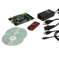
DV164136 Microchip Technology, DV164136 Datasheet - Page 160

DV164136
Manufacturer Part Number
DV164136
Description
DEVELOPMENT KIT FOR PIC18
Manufacturer
Microchip Technology
Series
PIC®r
Type
MCUr
Datasheets
1.DM183032.pdf
(38 pages)
2.DV164136.pdf
(448 pages)
3.DV164136.pdf
(6 pages)
4.DV164136.pdf
(446 pages)
5.DV164136.pdf
(4 pages)
6.DV164136.pdf
(18 pages)
Specifications of DV164136
Contents
Board, Cables, CDs, PICkit™ 3 Programmer, Power Supply
Processor To Be Evaluated
PIC18F8722, PIC18F87J11
Interface Type
RS-232, USB
Operating Supply Voltage
3.3 V, 5 V
Silicon Manufacturer
Microchip
Core Architecture
PIC
Core Sub-architecture
PIC18
Silicon Core Number
PIC18F
Silicon Family Name
PIC18F8xxx
Kit Contents
PIC18 Exp Brd PICkit 3 Cable CD PSU
Lead Free Status / RoHS Status
Lead free / RoHS Compliant
For Use With/related Products
PIC18F8722, PIC18F87J11
Lead Free Status / Rohs Status
Lead free / RoHS Compliant
Available stocks
Company
Part Number
Manufacturer
Quantity
Price
Company:
Part Number:
DV164136
Manufacturer:
MICROCHIP
Quantity:
12 000
- DM183032 PDF datasheet
- DV164136 PDF datasheet #2
- DV164136 PDF datasheet #3
- DV164136 PDF datasheet #4
- DV164136 PDF datasheet #5
- DV164136 PDF datasheet #6
- Current page: 160 of 448
- Download datasheet (8Mb)
PIC18F87J11 FAMILY
11.1.2
The PMP module uses 6 registers for transferring data
into and out of the microcontroller. They are arranged
as three pairs to allow the option of 16-bit data
operations:
• PMDIN1H and PMDIN1L
• PMDIN2H and PMDIN2L
• PMADDRH/PMDOUT1H and PMADDRL/PMDOUT1L
• PMDOUT2H and PMDOUT2L
The PMDIN1 register is used for incoming data in Slave
modes, and both input and output data in Master
modes. The PMDIN2 register is used for buffering input
data in select Slave modes.
The PMADDRx/PMDOUT1x registers are actually a
single register pair; the name and function is dictated
by the module’s operating mode. In Master modes, the
registers functions as the PMADDRH and PMADDRL
registers, and contain the address of any incoming or
outgoing data. In Slave modes, the registers function
as PMDOUT1H and PMDOUT1L and are used for
outgoing data.
PMADDRH differs from PMADDRL in that it can also
have limited PMP control functions. When the module
is operating in select Master mode configurations, the
REGISTER 11-9:
DS39778D-page 160
bit 7
Legend:
R = Readable bit
-n = Value at Reset
bit 7
bit 6
bit 5-0
Note 1:
R/W-0
CS2
In Enhanced Slave mode, PMADDRH functions as PMDOUT1H, one of the Output Data Buffer registers.
DATA REGISTERS
CS2: Chip Select 2 bit
If PMCON<7:6> = 10 or 01:
1 = Chip Select 2 is active
0 = Chip Select 2 is inactive
If PMCON<7:6> = 11 or 00:
Bit functions as ADDR<15>.
CS1: Chip Select 1 bit
If PMCON<7:6> = 10:
1 = Chip Select 1 is active
0 = Chip Select 1 is inactive
If PMCON<7:6> = 11 or 0x:
Bit functions as ADDR<14>.
ADDR13:ADDR0: Destination Address bits
R/W-0
CS1
PMADDRH: PARALLEL PORT ADDRESS REGISTER, HIGH BYTE
(MASTER MODES ONLY)
W = Writable bit
1 = bit is set
R/W-0
R/W-0
(1)
U = Unimplemented bit, read as ‘0’
0 = bit is cleared
R/W-0
upper two bits of the register can be used to determine
the operation of chip select signals. If chip select
signals are not used, PMADDR simply functions to hold
the upper 8 bits of the address. The function of the
individual bits in PMADDRH is shown in Register 11-9.
The PMDOUT2H and PMDOUT2L registers are only
used in buffered Slave modes and serve as a buffer for
outgoing data.
11.1.3
In addition to the module level configuration options,
the PMP module can also be configured at the I/O pin
for electrical operation. This option allows users to
select either the normal Schmitt Trigger input buffer on
digital I/O pins shared with the PMP, or use TTL level
compatible buffers instead. Buffer configuration is
controlled by the PMPTTL bit in the PADCFG1 register.
The PADCFG1 register is one of the shared address
SFRs, and has the same address as the TMR2 regis-
ter. PADCFG1 is accessed by setting the ADSHR bit
(WDTCON<4>). Refer to Section 5.3.4.1 “Shared
Address SFRs” for more information.
ADDR<13:8>
PAD CONFIGURATION CONTROL
REGISTER
R/W-0
© 2009 Microchip Technology Inc.
x = bit is unknown
R/W-0
R/W-0
bit 0
Related parts for DV164136
Image
Part Number
Description
Manufacturer
Datasheet
Request
R

Part Number:
Description:
Manufacturer:
Microchip Technology Inc.
Datasheet:

Part Number:
Description:
Manufacturer:
Microchip Technology Inc.
Datasheet:

Part Number:
Description:
Manufacturer:
Microchip Technology Inc.
Datasheet:

Part Number:
Description:
Manufacturer:
Microchip Technology Inc.
Datasheet:

Part Number:
Description:
Manufacturer:
Microchip Technology Inc.
Datasheet:

Part Number:
Description:
Manufacturer:
Microchip Technology Inc.
Datasheet:

Part Number:
Description:
Manufacturer:
Microchip Technology Inc.
Datasheet:

Part Number:
Description:
Manufacturer:
Microchip Technology Inc.
Datasheet:


