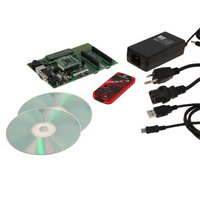
DV164136 Microchip Technology, DV164136 Datasheet - Page 192

DV164136
Manufacturer Part Number
DV164136
Description
DEVELOPMENT KIT FOR PIC18
Manufacturer
Microchip Technology
Series
PIC®r
Type
MCUr
Datasheets
1.DM183032.pdf
(38 pages)
2.DV164136.pdf
(448 pages)
3.DV164136.pdf
(6 pages)
4.DV164136.pdf
(446 pages)
5.DV164136.pdf
(4 pages)
6.DV164136.pdf
(18 pages)
Specifications of DV164136
Contents
Board, Cables, CDs, PICkit™ 3 Programmer, Power Supply
Processor To Be Evaluated
PIC18F8722, PIC18F87J11
Interface Type
RS-232, USB
Operating Supply Voltage
3.3 V, 5 V
Silicon Manufacturer
Microchip
Core Architecture
PIC
Core Sub-architecture
PIC18
Silicon Core Number
PIC18F
Silicon Family Name
PIC18F8xxx
Kit Contents
PIC18 Exp Brd PICkit 3 Cable CD PSU
Lead Free Status / RoHS Status
Lead free / RoHS Compliant
For Use With/related Products
PIC18F8722, PIC18F87J11
Lead Free Status / Rohs Status
Lead free / RoHS Compliant
Available stocks
Company
Part Number
Manufacturer
Quantity
Price
Company:
Part Number:
DV164136
Manufacturer:
MICROCHIP
Quantity:
12 000
- DM183032 PDF datasheet
- DV164136 PDF datasheet #2
- DV164136 PDF datasheet #3
- DV164136 PDF datasheet #4
- DV164136 PDF datasheet #5
- DV164136 PDF datasheet #6
- Current page: 192 of 448
- Download datasheet (8Mb)
PIC18F87J11 FAMILY
15.1
Timer3 can operate in one of three modes:
• Timer
• Synchronous Counter
• Asynchronous Counter
FIGURE 15-1:
FIGURE 15-2:
DS39778D-page 192
Note 1: When enable bit, T1OSCEN, is cleared, the inverter and feedback resistor are turned off to eliminate power drain.
Note 1: When enable bit, T1OSCEN, is cleared, the inverter and feedback resistor are turned off to eliminate power drain.
T1OSO/T13CKI
T13CKI/T1OSO
Timer3 Operation
T1OSI
T1OSI
ECCPx/CCPx Select from T3CON<6,3>
ECCPx/CCPx Select from T3CON<6,3>
ECCPx Special Event Trigger
ECCPx Special Event Trigger
Timer1 Oscillator
Timer1 Oscillator
T1OSCEN
T3CKPS1:T3CKPS0
T3SYNC
TMR3ON
TIMER3 BLOCK DIAGRAM
T1OSCEN
T3CKPS1:T3CKPS0
T3SYNC
TMR3ON
TIMER3 BLOCK DIAGRAM (16-BIT READ/WRITE MODE)
(1)
(1)
TMR3CS
TMR3CS
Clock
Internal
F
Internal
Clock
F
OSC
OSC
/4
/4
1
0
1
0
Timer1 Clock Input
Timer1 Clock Input
Clear TMR3
Clear TMR3
Prescaler
Prescaler
1, 2, 4, 8
1, 2, 4, 8
The operating mode is determined by the clock select
bit, TMR3CS (T3CON<1>). When TMR3CS is cleared
(= 0), Timer3 increments on every internal instruction
cycle (F
on every rising edge of the Timer1 external clock input
or the Timer1 oscillator, if enabled.
As
RC0/T1OSO/T13CKI pins become inputs when the
Timer1 oscillator is enabled. This means the values of
TRISC<1:0> are ignored and the pins are read as ‘0’.
2
2
with
OSC
TMR3L
TMR3L
/4). When the bit is set, Timer3 increments
8
Timer1,
8
Synchronize
Synchronize
Sleep Input
Sleep Input
Detect
Detect
High Byte
High Byte
TMR3H
TMR3
TMR3
8
© 2009 Microchip Technology Inc.
8
the
8
Internal Data Bus
1
0
1
0
Read TMR1L
Write TMR1L
RC1/T1OSI
Set
TMR3IF
on Overflow
Set
TMR3IF
on Overflow
Timer3
On/Off
Timer3
On/Off
and
Related parts for DV164136
Image
Part Number
Description
Manufacturer
Datasheet
Request
R

Part Number:
Description:
Manufacturer:
Microchip Technology Inc.
Datasheet:

Part Number:
Description:
Manufacturer:
Microchip Technology Inc.
Datasheet:

Part Number:
Description:
Manufacturer:
Microchip Technology Inc.
Datasheet:

Part Number:
Description:
Manufacturer:
Microchip Technology Inc.
Datasheet:

Part Number:
Description:
Manufacturer:
Microchip Technology Inc.
Datasheet:

Part Number:
Description:
Manufacturer:
Microchip Technology Inc.
Datasheet:

Part Number:
Description:
Manufacturer:
Microchip Technology Inc.
Datasheet:

Part Number:
Description:
Manufacturer:
Microchip Technology Inc.
Datasheet:


