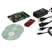
DV164136 Microchip Technology, DV164136 Datasheet - Page 206

DV164136
Manufacturer Part Number
DV164136
Description
DEVELOPMENT KIT FOR PIC18
Manufacturer
Microchip Technology
Series
PIC®r
Type
MCUr
Datasheets
1.DM183032.pdf
(38 pages)
2.DV164136.pdf
(448 pages)
3.DV164136.pdf
(6 pages)
4.DV164136.pdf
(446 pages)
5.DV164136.pdf
(4 pages)
6.DV164136.pdf
(18 pages)
Specifications of DV164136
Contents
Board, Cables, CDs, PICkit™ 3 Programmer, Power Supply
Processor To Be Evaluated
PIC18F8722, PIC18F87J11
Interface Type
RS-232, USB
Operating Supply Voltage
3.3 V, 5 V
Silicon Manufacturer
Microchip
Core Architecture
PIC
Core Sub-architecture
PIC18
Silicon Core Number
PIC18F
Silicon Family Name
PIC18F8xxx
Kit Contents
PIC18 Exp Brd PICkit 3 Cable CD PSU
Lead Free Status / RoHS Status
Lead free / RoHS Compliant
For Use With/related Products
PIC18F8722, PIC18F87J11
Lead Free Status / Rohs Status
Lead free / RoHS Compliant
Available stocks
Company
Part Number
Manufacturer
Quantity
Price
Company:
Part Number:
DV164136
Manufacturer:
MICROCHIP
Quantity:
12 000
- DM183032 PDF datasheet
- DV164136 PDF datasheet #2
- DV164136 PDF datasheet #3
- DV164136 PDF datasheet #4
- DV164136 PDF datasheet #5
- DV164136 PDF datasheet #6
- Current page: 206 of 448
- Download datasheet (8Mb)
PIC18F87J11 FAMILY
REGISTER 18-1:
18.1
Each of the Enhanced CCP modules may have up to
four PWM outputs, depending on the selected
operating mode. These outputs, designated PxA
through PxD, are multiplexed with various I/O pins.
Some ECCP pin assignments are constant, while
others change based on device configuration. For
those pins that do change, the controlling bits are:
• CCP2MX Configuration bit
• ECCPMX Configuration bit (80-pin devices only)
• Program Memory Operating mode, set by the
The pin assignments for the Enhanced CCP modules
are summarized in Table 18-1, Table 18-2 and
Table 18-3. To configure the I/O pins as PWM outputs,
the proper PWM mode must be selected by setting the
PxMx and CCPxMx bits (CCPxCON<7:6> and <3:0>,
respectively). The appropriate TRIS direction bits for
the corresponding port pins must also be set as
outputs.
18.1.1
In 80-pin devices, the use of Extended Microcontroller
mode has an indirect effect on the use of ECCP1 and
ECCP3 in Enhanced PWM modes. By default, PWM
outputs, P1B/P1C and P3B/P3C, are multiplexed to
PORTE pins along with the high-order byte of the
external memory bus. When the bus is active in
Extended Microcontroller mode, it overrides the
Enhanced CCP outputs and makes them unavailable.
Because of this, ECCP1 and ECCP3 can only be used
in compatible (single output) PWM modes when the
device is in Extended Microcontroller mode and default
pin configuration.
DS39778D-page 206
bit 3-0
EMB Configuration bits (80-pin devices only)
ECCP Outputs and Configuration
ECCP1/ECCP3 OUTPUTS AND
PROGRAM MEMORY MODE
CCPxM3:CCPxM0: Enhanced CCPx Module Mode Select bits
0000 = Capture/Compare/PWM off (resets ECCPx module)
0001 = Reserved
0010 = Compare mode, toggle output on match
0011 = Capture mode
0100 = Capture mode: every falling edge
0101 = Capture mode: every rising edge
0110 = Capture mode: every 4th rising edge
0111 = Capture mode: every 16th rising edge
1000 = Compare mode: initialize ECCPx pin low; set output on compare match (set CCPxIF)
1001 = Compare mode: initialize ECCPx pin high; clear output on compare match (set CCPxIF)
1010 = Compare mode: generate software interrupt only; ECCPx pin reverts to I/O state
1011 = Compare mode: trigger special event (ECCPx resets TMR1 or TMR3, sets CCPxIF bit,
1100 = PWM mode: PxA, PxC active-high; PxB, PxD active-high
1101 = PWM mode: PxA, PxC active-high; PxB, PxD active-low
1110 = PWM mode: PxA, PxC active-low; PxB, PxD active-high
1111 = PWM mode: PxA, PxC active-low; PxB, PxD active-low
Note 1:
CCPxCON: ECCPx CONTROL REGISTER (ECCP1/ECCP2/ECCP3)
ECCPx trigger also starts A/D conversion if A/D module is enabled)
Implemented only for ECCP1 and ECCP2; same as ‘1010’ for ECCP3.
An exception to this configuration is when a 12-bit
address width is selected for the external bus
(EMB1:EMB0 Configuration bits = 01). In this case, the
upper pins of PORTE continue to operate as digital I/O,
even when the external bus is active. P1B/P1C and
P3B/P3C remain available for use as Enhanced PWM
outputs.
If an application requires the use of additional PWM
outputs during enhanced microcontroller operation, the
P1B/P1C and P3B/P3C outputs can be reassigned to
the upper bits of PORTH. This is done by clearing the
ECCPMX Configuration bit.
18.1.2
For 80-pin devices, the program memory mode of the
device (Section 5.1.3 “PIC18F8xJ11/8XJ16 Program
Memory Modes”) also impacts pin multiplexing for the
module.
The ECCP2 input/output (ECCP2/P2A) can be
multiplexed to one of three pins. The default
assignment (CCP2MX Configuration bit is set) for all
devices is RC1. Clearing CCP2MX reassigns ECCP2/
P2A to RE7.
An additional option exists for 80-pin devices. When
these devices are operating in Microcontroller mode,
the multiplexing options described above still apply. In
Extended Microcontroller mode, clearing CCP2MX
reassigns ECCP2/P2A to RB3.
Changing the pin assignment of ECCP2 does not
automatically change any requirements for configuring
the port pin. Users must always verify that the
appropriate TRIS register is configured correctly for
ECCP2 operation regardless of where it is located.
ECCP2 OUTPUTS AND PROGRAM
MEMORY MODES
(1)
© 2009 Microchip Technology Inc.
Related parts for DV164136
Image
Part Number
Description
Manufacturer
Datasheet
Request
R

Part Number:
Description:
Manufacturer:
Microchip Technology Inc.
Datasheet:

Part Number:
Description:
Manufacturer:
Microchip Technology Inc.
Datasheet:

Part Number:
Description:
Manufacturer:
Microchip Technology Inc.
Datasheet:

Part Number:
Description:
Manufacturer:
Microchip Technology Inc.
Datasheet:

Part Number:
Description:
Manufacturer:
Microchip Technology Inc.
Datasheet:

Part Number:
Description:
Manufacturer:
Microchip Technology Inc.
Datasheet:

Part Number:
Description:
Manufacturer:
Microchip Technology Inc.
Datasheet:

Part Number:
Description:
Manufacturer:
Microchip Technology Inc.
Datasheet:


