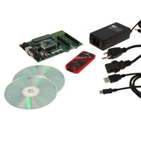
DV164136 Microchip Technology, DV164136 Datasheet - Page 237

DV164136
Manufacturer Part Number
DV164136
Description
DEVELOPMENT KIT FOR PIC18
Manufacturer
Microchip Technology
Series
PIC®r
Type
MCUr
Datasheets
1.DM183032.pdf
(38 pages)
2.DV164136.pdf
(448 pages)
3.DV164136.pdf
(6 pages)
4.DV164136.pdf
(446 pages)
5.DV164136.pdf
(4 pages)
6.DV164136.pdf
(18 pages)
Specifications of DV164136
Contents
Board, Cables, CDs, PICkit™ 3 Programmer, Power Supply
Processor To Be Evaluated
PIC18F8722, PIC18F87J11
Interface Type
RS-232, USB
Operating Supply Voltage
3.3 V, 5 V
Silicon Manufacturer
Microchip
Core Architecture
PIC
Core Sub-architecture
PIC18
Silicon Core Number
PIC18F
Silicon Family Name
PIC18F8xxx
Kit Contents
PIC18 Exp Brd PICkit 3 Cable CD PSU
Lead Free Status / RoHS Status
Lead free / RoHS Compliant
For Use With/related Products
PIC18F8722, PIC18F87J11
Lead Free Status / Rohs Status
Lead free / RoHS Compliant
Available stocks
Company
Part Number
Manufacturer
Quantity
Price
Company:
Part Number:
DV164136
Manufacturer:
MICROCHIP
Quantity:
12 000
- DM183032 PDF datasheet
- DV164136 PDF datasheet #2
- DV164136 PDF datasheet #3
- DV164136 PDF datasheet #4
- DV164136 PDF datasheet #5
- DV164136 PDF datasheet #6
- Current page: 237 of 448
- Download datasheet (8Mb)
REGISTER 19-6:
REGISTER 19-7:
© 2009 Microchip Technology Inc.
bit 7
Legend:
R = Readable bit
-n = Value at POR
bit 7
bit 6
bit 5-2
bit 1
bit 0
Note 1:
bit 7
Legend:
R = Readable bit
-n = Value at POR
bit 7-0
Note 1:
R/W-0
GCEN
R/W-1
MSK7
2:
If the I
writes to the SSPxBUF are disabled).
This register shares the same SFR address as SSPxADD, and is only addressable in select MSSPx
operating modes. See Section 19.4.3.4 “7-Bit Address Masking Mode” for more details.
MSK0 is not used as a mask bit in 7-bit addressing.
GCEN: General Call Enable bit
1 = Enables interrupt when a general call address (0000h) is received in the SSPSR
0 = General call address disabled
ACKSTAT: Acknowledge Status bit
Unused in Slave mode.
ADMSK5:ADMSK2: Slave Address Mask Select bits (5-Bit Address Masking mode)
1 = Masking of corresponding bits of SSPxADD enabled
0 = Masking of corresponding bits of SSPxADD disabled
ADMSK1: Slave Address Least Significant bit(s) Mask Select bit
In 7-Bit Addressing mode:
1 = Masking of SSPxADD<1> only enabled
0 = Masking of SSPxADD<1> only disabled
In 10-Bit Addressing mode:
1 = Masking of SSPxADD<1:0> enabled
0 = Masking of SSPxADD<1:0> disabled
SEN: Stretch Enable bit
1 = Clock stretching is enabled for both slave transmit and slave receive (stretch enabled)
0 = Clock stretching is disabled
MSK7:MSK0: Slave Address Mask Select bit
1 = Masking of corresponding bit of SSPxADD enabled
0 = Masking of corresponding bit of SSPxADD disabled
ACKSTAT
2
R/W-0
C module is active, this bit may not be set (no spooling) and the SSPBUF may not be written (or
R/W-1
MSK6
SSPxCON2: MSSPx CONTROL REGISTER 2 (I
SSPxMSK: I
W = Writable bit
‘1’ = Bit is set
W = Writable bit
‘1’ = Bit is set
ADMSK5
R/W-0
R/W-1
MSK5
2
C™ SLAVE ADDRESS MASK REGISTER (7-BIT MASKING MODE)
(1)
ADMSK4
R/W-0
R/W-1
MSK4
U = Unimplemented bit, read as ‘0’
‘0’ = Bit is cleared
U = Unimplemented bit, read as ‘0’
‘0’ = Bit is cleared
ADMSK3
PIC18F87J11 FAMILY
R/W-0
R/W-1
MSK3
ADMSK2
2
R/W-0
R/W-1
MSK2
C™ SLAVE MODE)
x = Bit is unknown
x = Bit is unknown
ADMSK1
R/W-0
R/W-1
MSK1
DS39778D-page 237
MSK0
SEN
R/W-0
R/W-1
(1)
(2)
bit 0
bit 0
(1)
Related parts for DV164136
Image
Part Number
Description
Manufacturer
Datasheet
Request
R

Part Number:
Description:
Manufacturer:
Microchip Technology Inc.
Datasheet:

Part Number:
Description:
Manufacturer:
Microchip Technology Inc.
Datasheet:

Part Number:
Description:
Manufacturer:
Microchip Technology Inc.
Datasheet:

Part Number:
Description:
Manufacturer:
Microchip Technology Inc.
Datasheet:

Part Number:
Description:
Manufacturer:
Microchip Technology Inc.
Datasheet:

Part Number:
Description:
Manufacturer:
Microchip Technology Inc.
Datasheet:

Part Number:
Description:
Manufacturer:
Microchip Technology Inc.
Datasheet:

Part Number:
Description:
Manufacturer:
Microchip Technology Inc.
Datasheet:


