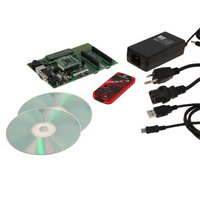
DV164136 Microchip Technology, DV164136 Datasheet - Page 107

DV164136
Manufacturer Part Number
DV164136
Description
DEVELOPMENT KIT FOR PIC18
Manufacturer
Microchip Technology
Series
PIC®r
Type
MCUr
Datasheets
1.DM183032.pdf
(38 pages)
2.DV164136.pdf
(448 pages)
3.DV164136.pdf
(6 pages)
4.DV164136.pdf
(446 pages)
5.DV164136.pdf
(4 pages)
6.DV164136.pdf
(18 pages)
Specifications of DV164136
Contents
Board, Cables, CDs, PICkit™ 3 Programmer, Power Supply
Processor To Be Evaluated
PIC18F8722, PIC18F87J11
Interface Type
RS-232, USB
Operating Supply Voltage
3.3 V, 5 V
Silicon Manufacturer
Microchip
Core Architecture
PIC
Core Sub-architecture
PIC18
Silicon Core Number
PIC18F
Silicon Family Name
PIC18F8xxx
Kit Contents
PIC18 Exp Brd PICkit 3 Cable CD PSU
Lead Free Status / RoHS Status
Lead free / RoHS Compliant
For Use With/related Products
PIC18F8722, PIC18F87J11
Lead Free Status / Rohs Status
Lead free / RoHS Compliant
Available stocks
Company
Part Number
Manufacturer
Quantity
Price
Company:
Part Number:
DV164136
Manufacturer:
MICROCHIP
Quantity:
12 000
- DM183032 PDF datasheet
- DV164136 PDF datasheet #2
- DV164136 PDF datasheet #3
- DV164136 PDF datasheet #4
- DV164136 PDF datasheet #5
- DV164136 PDF datasheet #6
- Current page: 107 of 448
- Download datasheet (8Mb)
7.7
In 8-Bit Data Width mode, the external memory bus
operates only in Multiplexed mode; that is, data shares
the 8 Least Significant bits of the address bus.
Figure 7-6 shows an example of 8-Bit Multiplexed
mode for 80-pin devices. This mode is used for a single
8-bit memory connected for 16-bit operation. The
instructions will be fetched as two 8-bit bytes on a
shared data/address bus. The two bytes are sequen-
tially fetched within one instruction cycle (T
Therefore, the designer must choose external memory
devices according to timing calculations based on
1/2 T
ory speed selection, glue logic propagation delay times
must be considered, along with setup and hold times.
The Address Latch Enable (ALE) pin indicates that the
address bits, AD<15:0>, are available on the external
memory interface bus. The Output Enable signal (OE)
FIGURE 7-6:
© 2009 Microchip Technology Inc.
CY
(2 times the instruction rate). For proper mem-
8-Bit Data Width Mode
Note 1:
2:
PIC18F87J11
Upper order address bits are only used for 20-bit address width. The upper AD byte is used for all
address widths except 8-bit.
This signal only applies to table writes. See Section 6.1 “Table Reads and Table Writes”.
AD<15:8>
A<19:16>
8-BIT MULTIPLEXED MODE EXAMPLE
AD<7:0>
WRL
ALE
BA0
CE
OE
(1)
(1)
CY
).
373
PIC18F87J11 FAMILY
will enable one byte of program memory for a portion of
the instruction cycle, then BA0 will change and the
second byte will be enabled to form the 16-bit instruc-
tion word. The Least Significant bit of the address, BA0,
must be connected to the memory devices in this
mode. The Chip Enable signal (CE) is active at any
time that the microcontroller accesses external
memory, whether reading or writing. It is inactive
(asserted high) whenever the device is in Sleep mode.
This generally includes basic EPROM and Flash
devices. It allows table writes to byte-wide external
memories.
During a TBLWT instruction cycle, the TABLAT data is
presented on the upper and lower bytes of the
AD15:AD0 bus. The appropriate level of the BA0
control line is strobed on the LSb of the TBLPTR.
D<7:0>
A<19:0>
D<15:8>
Address Bus
Data Bus
Control Lines
A0
OE
A<x:1>
D<7:0>
CE
WR
DS39778D-page 107
(2)
Related parts for DV164136
Image
Part Number
Description
Manufacturer
Datasheet
Request
R

Part Number:
Description:
Manufacturer:
Microchip Technology Inc.
Datasheet:

Part Number:
Description:
Manufacturer:
Microchip Technology Inc.
Datasheet:

Part Number:
Description:
Manufacturer:
Microchip Technology Inc.
Datasheet:

Part Number:
Description:
Manufacturer:
Microchip Technology Inc.
Datasheet:

Part Number:
Description:
Manufacturer:
Microchip Technology Inc.
Datasheet:

Part Number:
Description:
Manufacturer:
Microchip Technology Inc.
Datasheet:

Part Number:
Description:
Manufacturer:
Microchip Technology Inc.
Datasheet:

Part Number:
Description:
Manufacturer:
Microchip Technology Inc.
Datasheet:


