DV164136 Microchip Technology, DV164136 Datasheet - Page 295

DV164136
Manufacturer Part Number
DV164136
Description
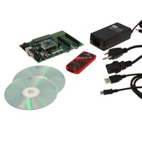
DEVELOPMENT KIT FOR PIC18
Manufacturer
Microchip Technology
Series
PIC®r
Type
MCUr
Datasheets
1.DM183032.pdf
(38 pages)
2.DV164136.pdf
(448 pages)
3.DV164136.pdf
(6 pages)
4.DV164136.pdf
(446 pages)
5.DV164136.pdf
(4 pages)
6.DV164136.pdf
(18 pages)
Specifications of DV164136
Contents
Board, Cables, CDs, PICkit™ 3 Programmer, Power Supply
Processor To Be Evaluated
PIC18F8722, PIC18F87J11
Interface Type
RS-232, USB
Operating Supply Voltage
3.3 V, 5 V
Silicon Manufacturer
Microchip
Core Architecture
PIC
Core Sub-architecture
PIC18
Silicon Core Number
PIC18F
Silicon Family Name
PIC18F8xxx
Kit Contents
PIC18 Exp Brd PICkit 3 Cable CD PSU
Lead Free Status / RoHS Status
Lead free / RoHS Compliant
For Use With/related Products
PIC18F8722, PIC18F87J11
Lead Free Status / Rohs Status
Lead free / RoHS Compliant
Available stocks
Company
Part Number
Manufacturer
Quantity
Price
Company:
Part Number:
DV164136
Manufacturer:
MICROCHIP
Quantity:
12 000
- DM183032 PDF datasheet
- DV164136 PDF datasheet #2
- DV164136 PDF datasheet #3
- DV164136 PDF datasheet #4
- DV164136 PDF datasheet #5
- DV164136 PDF datasheet #6
- Current page: 295 of 448
- Download datasheet (8Mb)
The ANCON0 and ANCON1 registers are used to
configure the operation of the I/O pin associated with
each analog channel. Setting any one of the PCFG bits
configures the corresponding pin to operate as a digital
only I/O. Clearing a bit configures the pin to operate as
an analog input for either the A/D Converter or the
comparator module; all digital peripherals are disabled,
and digital inputs read as ‘0’. As a rule, I/O pins that are
multiplexed with analog inputs default to analog
operation on device Resets.
REGISTER 21-3:
REGISTER 21-4:
© 2009 Microchip Technology Inc.
bit 7
Legend:
R = Readable bit
-n = Value at POR
bit 7-6
bit 5
bit 4-0
bit 7
Legend:
R = Readable bit
-n = Value at POR
bit 7-0
Note 1:
PCFG15
PCFG7
R/W-0
R/W-0
(1)
AN15 through AN12 are implemented only on 80-pin devices. For 64-pin devices, the corresponding
PCFGx bits are still implemented for these channels, but have no effect.
PCFG7:PCFG6: Analog Port Configuration bits (AN7 and AN6)
1 = Pin configured as a digital port
0 = Pin configured as an analog channel; digital input disabled and reads ‘0’
Unimplemented: Read as ‘0’
PCFG4:PCFG0: Analog Port Configuration bits (AN4 through AN0)
1 = Pin configured as a digital port
0 = Pin configured as an analog channel; digital input disabled and reads ‘0’
PCFG15:PCFG8: Analog Port Configuration bits (AN15 through AN8)
1 = Pin configured as a digital port
0 = Pin configured as an analog channel; digital input disabled and reads ‘0’
PCFG14
PCFG6
R/W-0
R/W-0
ANCON0: A/D PORT CONFIGURATION REGISTER 2
ANCON1: A/D PORT CONFIGURATION REGISTER 1
(1)
W = Writable bit
W = Writable bit
‘1’ = Bit is set
‘1’ = Bit is set
PCFG13
R/W-0
U-0
—
(1)
PCFG12
PCFG4
R/W-0
R/W-0
(1)
U = Unimplemented bit, read as ‘0’
‘0’ = Bit is cleared
U = Unimplemented bit, read as ‘0’
‘0’ = Bit is cleared
PIC18F87J11 FAMILY
PCFG11
PCFG3
R/W-0
R/W-0
ANCON0 and ANCON1 are shared address SFRs, and
use the same addresses as the ADCON1 and
ADCON0 registers. The ANCON registers are
accessed by setting the ADSHR bit (WDTCON<4>).
See Section 5.3.4.1 “Shared Address SFRs” for
more information.
PCFG10
PCFG2
R/W-0
R/W-0
x = Bit is unknown
x = Bit is unknown
PCFG1
PCFG9
R/W-0
R/W-0
DS39778D-page 295
PCFG0
PCFG8
R/W-0
R/W-0
bit 0
bit 0
Related parts for DV164136
Image
Part Number
Description
Manufacturer
Datasheet
Request
R

Part Number:
Description:
Manufacturer:
Microchip Technology Inc.
Datasheet:

Part Number:
Description:
Manufacturer:
Microchip Technology Inc.
Datasheet:

Part Number:
Description:
Manufacturer:
Microchip Technology Inc.
Datasheet:

Part Number:
Description:
Manufacturer:
Microchip Technology Inc.
Datasheet:

Part Number:
Description:
Manufacturer:
Microchip Technology Inc.
Datasheet:

Part Number:
Description:
Manufacturer:
Microchip Technology Inc.
Datasheet:

Part Number:
Description:
Manufacturer:
Microchip Technology Inc.
Datasheet:

Part Number:
Description:
Manufacturer:
Microchip Technology Inc.
Datasheet:


