DV164136 Microchip Technology, DV164136 Datasheet - Page 207

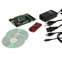
DV164136
Manufacturer Part Number
DV164136
Description
DEVELOPMENT KIT FOR PIC18
Manufacturer
Microchip Technology
Series
PIC®r
Type
MCUr
Datasheets
1.DM183032.pdf
(38 pages)
2.DV164136.pdf
(448 pages)
3.DV164136.pdf
(6 pages)
4.DV164136.pdf
(446 pages)
5.DV164136.pdf
(4 pages)
6.DV164136.pdf
(18 pages)
Specifications of DV164136
Contents
Board, Cables, CDs, PICkit™ 3 Programmer, Power Supply
Processor To Be Evaluated
PIC18F8722, PIC18F87J11
Interface Type
RS-232, USB
Operating Supply Voltage
3.3 V, 5 V
Silicon Manufacturer
Microchip
Core Architecture
PIC
Core Sub-architecture
PIC18
Silicon Core Number
PIC18F
Silicon Family Name
PIC18F8xxx
Kit Contents
PIC18 Exp Brd PICkit 3 Cable CD PSU
Lead Free Status / RoHS Status
Lead free / RoHS Compliant
For Use With/related Products
PIC18F8722, PIC18F87J11
Lead Free Status / Rohs Status
Lead free / RoHS Compliant
Available stocks
Company
Part Number
Manufacturer
Quantity
Price
Company:
Part Number:
DV164136
Manufacturer:
MICROCHIP
Quantity:
12 000
- DM183032 PDF datasheet
- DV164136 PDF datasheet #2
- DV164136 PDF datasheet #3
- DV164136 PDF datasheet #4
- DV164136 PDF datasheet #5
- DV164136 PDF datasheet #6
- Current page: 207 of 448
- Download datasheet (8Mb)
18.1.3
Only the ECCP2 module has four dedicated output pins
that are available for use. Assuming that the I/O ports
or other multiplexed functions on those pins are not
needed, they may be used whenever needed without
interfering with any other CCP module.
ECCP1 and ECCP3, on the other hand, only have
three dedicated output pins: ECCPx/PxA, PxB and
PxC. Whenever these modules are configured for
Quad PWM mode, the pin normally used for CCP4 or
CCP5 becomes the PxD output pins for ECCP3 and
ECCP1, respectively. The CCP4 and CCP5 modules
remain functional but their outputs are overridden.
18.1.4
Like the standard CCP modules, the ECCP modules
can utilize Timers 1, 2, 3 or 4, depending on the mode
selected. Timer1 and Timer3 are available for modules
in Capture or Compare modes, while Timer2 and
Timer4 are available for modules in PWM mode.
Additional details on timer resources are provided in
Section 17.1.1
Resources”.
TABLE 18-1:
© 2009 Microchip Technology Inc.
Compatible CCP
Dual PWM
Quad PWM
Compatible CCP
Dual PWM
Quad PWM
Compatible CCP
Compatible CCP
Dual PWM
Quad PWM
Legend: x = Don’t care, N/A = Not Available. Shaded cells indicate pin assignments not used by ECCP1 in a given mode.
Note 1:
ECCP Mode
PIC18F8XJ1X Devices, ECCPMX = 1, Extended Microcontroller mode, 16-Bit or 20-Bit Address Width:
With ECCP1 in Quad PWM mode, CCP5’s output is overridden by P1D; otherwise, CCP5 is fully operational.
USE OF CCP4 AND CCP5 WITH
ECCP1 AND ECCP3
ECCP MODULES AND TIMER
RESOURCES
(1)
(1)
(1)
Microcontroller mode or Extended Microcontroller mode, 12-Bit Address Width:
PIN CONFIGURATIONS FOR ECCP1
“CCP
Configuration
00xx 11xx
10xx 11xx
x1xx 11xx
00xx 11xx
10xx 11xx
x1xx 11xx
00xx 11xx
00xx 11xx
10xx 11xx
x1xx 11xx
CCP1CON
PIC18F8XJ1X Devices, ECCPMX = 0, Microcontroller mode:
Modules
ECCP1
ECCP1
ECCP1
ECCP1
RC2
P1A
P1A
P1A
P1A
P1A
P1A
PIC18F8XJ1X Devices, ECCPMX = 1,
and
All PIC18F6XJ1X Devices:
Timer
RE6/AD14
RE6/AD14
RE6/AD14
RE6/AD14
RE6/AD14
RE6
RE6
P1B
P1B
P1B
P1B
PIC18F87J11 FAMILY
18.1.5
When operating in compare or standard PWM modes,
the drivers for the ECCP pins can be optionally
configured as open-drain outputs. This feature allows
the voltage level on the pin to be pulled to a higher level
through an external pull-up resistor, and allows the
output to communicate with external circuits without the
need for additional level shifters. For more information,
see Section 10.1.4 “Open-Drain Outputs”
The open-drain output option is controlled by the bits in
the ODCON1 register. Setting the appropriate bit
configures the pin for the corresponding module for
open-drain operation. The ODCON1 memory shares
the same address space as of TMR1H. The ODCON1
register can be accessed by setting the ADSHR bit in
the WDTCON register (WDTCON<4>).
RE5/AD13
RE5/AD13
RE5/AD13
RE5/AD13
RE5/AD13
RE5/AD13
RE5
RE5
RE5
P1C
P1C
OPEN-DRAIN OUTPUT OPTION
RG4/CCP5
RG4/CCP5
RG4/CCP5
RG4/CCP5
RG4/CCP5
RG4/CCP5
RG4/CCP5
RG4
P1D
P1D
P1D
RH7/AN15
RH7/AN15
RH7/AN15
RH7/AN15
RH7/AN15
RH7
P1B
P1B
N/A
N/A
N/A
DS39778D-page 207
RH6/AN14
RH6/AN14
RH6/AN14
RH6/AN14
RH6/AN14
RH6/AN14
RH6
P1C
N/A
N/A
N/A
Related parts for DV164136
Image
Part Number
Description
Manufacturer
Datasheet
Request
R

Part Number:
Description:
Manufacturer:
Microchip Technology Inc.
Datasheet:

Part Number:
Description:
Manufacturer:
Microchip Technology Inc.
Datasheet:

Part Number:
Description:
Manufacturer:
Microchip Technology Inc.
Datasheet:

Part Number:
Description:
Manufacturer:
Microchip Technology Inc.
Datasheet:

Part Number:
Description:
Manufacturer:
Microchip Technology Inc.
Datasheet:

Part Number:
Description:
Manufacturer:
Microchip Technology Inc.
Datasheet:

Part Number:
Description:
Manufacturer:
Microchip Technology Inc.
Datasheet:

Part Number:
Description:
Manufacturer:
Microchip Technology Inc.
Datasheet:


